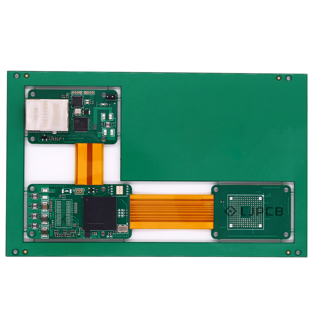
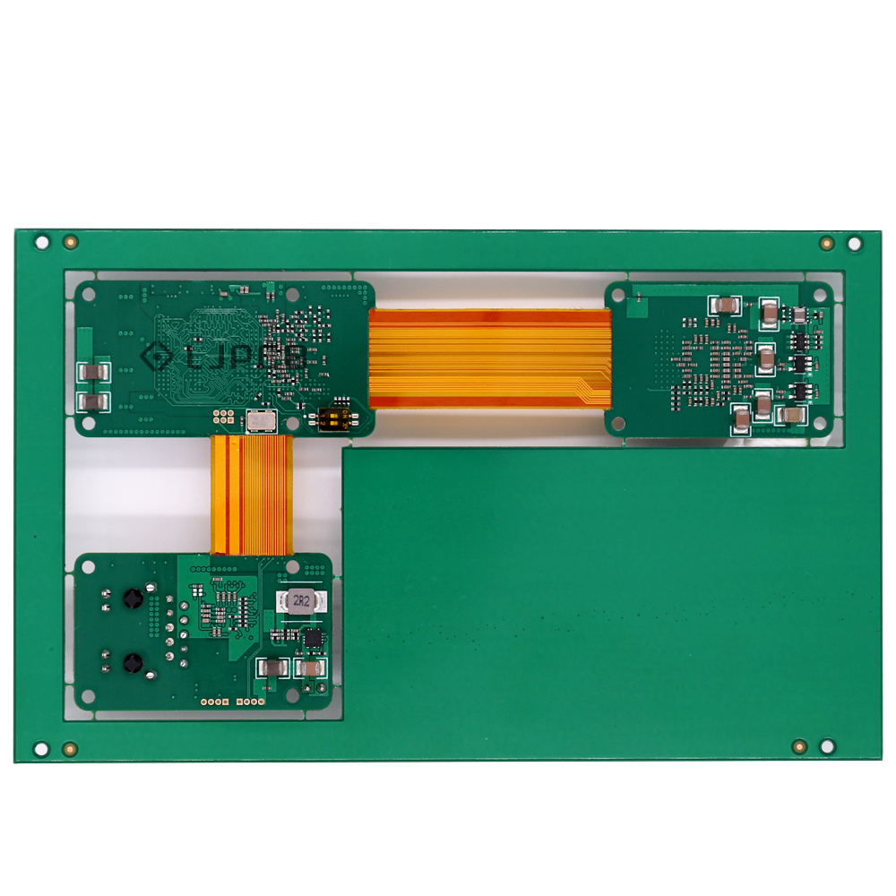
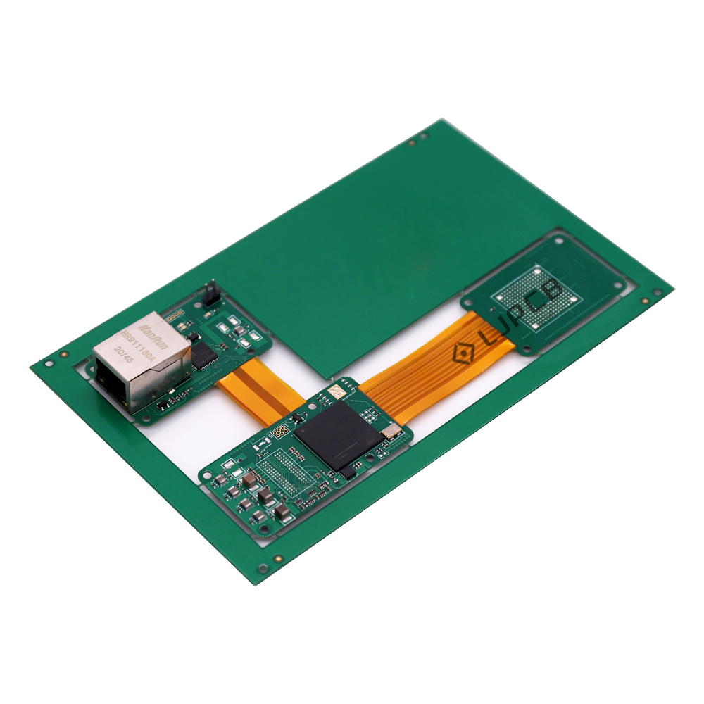
Description: This PCB is used as the module control board of a GigE area scan camera. It is designed to manage image acquisition, data processing, and Gigabit Ethernet communication within the camera module, enabling high-speed image transmission and stable system operation. The board integrates image processing circuits, communication interfaces, power management, and peripheral control functions to support reliable performance in machine vision, industrial inspection, and intelligent imaging applications. LJPCB provides one-stop turnkey
PCB assembly services, including PCB fabrication, component sourcing, SMT assembly, functional testing, and complete PCBA manufacturing solutions for industrial imaging equipment and embedded vision systems.
| Layer | 10L | Material Thickness | 1.6mm |
|---|
| Surface Finishing | ENIG | Finished Copper Thickness | 1oz |
|---|
| Solder Mask | Green | Legend Mark | White |
|---|
| Test | Test-Flying Probe | Routed OutLine/Punching | CNC+V-CUT |
|---|