

What is wave soldering?
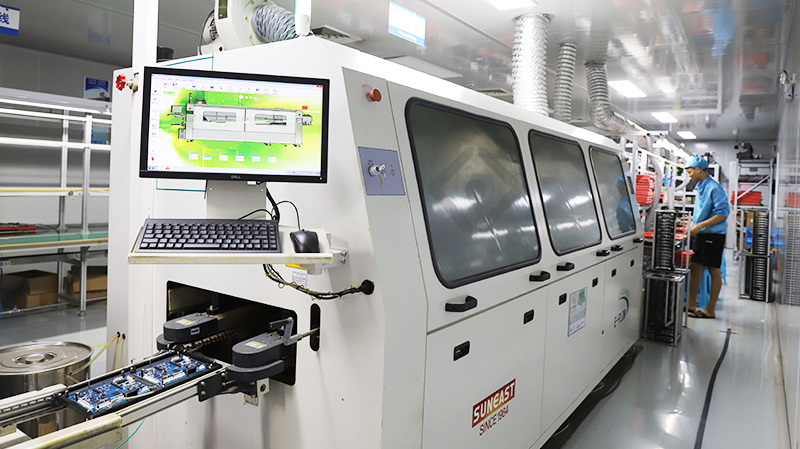
During PCB assembly, when a product contains large connectors, high-power components, or other through-hole components that require strong mechanical connections, wave soldering is often selected as an effective soldering solution. Let’s take a closer look at the wave soldering process and its applications.
Wave soldering requires specialized wave soldering equipment. Unlike the reflow soldering process, which melts solder paste on the PCB surface through controlled heating, wave soldering uses molten solder contained in a solder pot inside the machine. The solder is heated to a liquid state, and a pump system generates a continuous wave of molten solder.
During the process, a PCB with inserted through-hole components is transported through the wave soldering machine by a conveyor system. The bottom side of the PCB passes over and contacts the molten solder wave, allowing the solder to flow through the component leads and PCB holes. After cooling, solid solder joints are formed between the component leads and PCB pads.
The reason it is called "wave soldering" is that the molten solder surface is shaped into a controlled wave pattern through mechanical or electromagnetic pumping systems, allowing the solder to contact the PCB evenly and complete the soldering process.
The advantages of wave soldering mainly include the following points.
Firstly, wave soldering provides high production efficiency. Compared with manual soldering, automated wave soldering equipment can process a large number of PCB assemblies in a short period of time, significantly improving manufacturing efficiency and reducing labor costs.
Secondly, wave soldering provides consistent soldering quality. By accurately controlling parameters such as solder temperature, conveyor speed, and wave height, manufacturers can achieve stable solder joints and improve production consistency.
In addition, wave soldering creates strong mechanical and electrical connections between through-hole component leads and PCB pads. These solder joints typically provide excellent mechanical strength and resistance to vibration, thermal cycling, and mechanical stress, making wave soldering suitable for industrial electronics, automotive electronics, and other applications requiring high reliability.
However, wave soldering also has some limitations.
For example, the high soldering temperature requires careful control to prevent thermal damage to temperature-sensitive components. In addition, soldering parameters such as wave height, solder temperature, flux application, and conveyor speed must be properly adjusted according to different PCB designs and component types. Improper parameter settings may result in soldering defects such as insufficient solder, solder bridges, or component damage.
Overall, wave soldering remains an important and reliable soldering technology in PCB assembly manufacturing. Although SMT reflow soldering has become the dominant process for modern electronic assembly, wave soldering continues to play an essential role in DIP assembly and through-hole applications. With the continuous development of electronic products and manufacturing technologies, wave soldering processes will continue to be optimized to provide higher efficiency, reliability, and quality for the electronics industry.