

SMT Tombstoning: Causes, Effects, and Prevention Methods in PCB Assembly
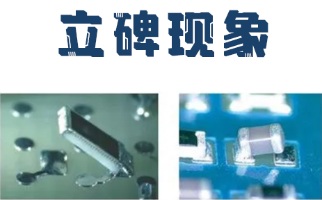
After years of working in PCB assembly, you will inevitably encounter a classic SMT defect: everything looks normal before the PCB enters the reflow oven—the stencil is fine, component placement is accurate, and the solder paste printing process appears perfect. However, after reflow soldering, resistors and capacitors suddenly stand up one after another like falling dominoes. This is one of the most well-known defects in the SMT industry—tombstoning.
In actual production, engineers may also refer to it as the “tombstone effect,� “drawbridge effect,� or more visually, the “Manhattan effect.� Although the names are different, they describe the same phenomenon: during the reflow soldering process, one end of a chip component remains soldered to the PCB pad while the other end lifts away from the pad, leaving the component standing upright like a tombstone.
Tombstoning mainly occurs on small chip components such as 0402 and 0201 packages. It is especially common with MLCC capacitors and miniature resistors, making it one of the key defects that must be controlled during SMT manufacturing.
Although tombstoning does not immediately cause obvious failures like short circuits or open circuits, it can result in component malfunction, reduced product reliability, and even affect the delivery quality of an entire batch of PCBA products. Therefore, reducing the occurrence rate of tombstoning has always been an important goal in SMT process control.
So, why does tombstoning happen, and how can it be prevented?
The fundamental cause of tombstoning is actually quite simple:
During the reflow soldering process, the solder on the two pads of a chip component does not melt at exactly the same time.
When the solder paste on one pad reaches the melting point first and becomes liquid, the surface tension of the molten solder quickly acts on the component terminal, generating an upward pulling force. If the solder on the opposite pad is still solid and cannot provide an equivalent balancing force, the component will be pulled toward the melted side by this uneven force, eventually causing it to lift up and form a tombstone defect.
This is the basic mechanism behind tombstoning.
Therefore, the key factor behind tombstoning is:
A difference in melting time between the two solder joints.
The greater the time difference, the more unbalanced the forces acting on both ends of the component become, increasing the probability of tombstoning.
The root cause of this melting time difference is:
Uneven temperature distribution between the two ends of the component.
When one pad reaches the solder melting point earlier while the other pad has not fully melted, surface tension becomes the dominant force and causes the component to tilt upward.
To understand why temperature differences lead to tombstoning, we first need to understand the standard reflow soldering process.
A typical reflow temperature profile consists of four stages:
1. Preheat Zone:
The temperature gradually rises from room temperature to approximately 150°C, with a typical ramp rate controlled between 1–3°C/s. This stage allows the PCB and components to heat evenly while activating the flux inside the solder paste. If the temperature rises too quickly, components may suffer from thermal shock and cracking.
2. Soak Zone:
The temperature is maintained between 150°C and 180°C for approximately 60–120 seconds. During this stage, the entire PCBA assembly reaches thermal equilibrium, the flux becomes fully activated, and oxides are removed from metal surfaces. This zone is critical for preventing tombstoning. If the soak time is insufficient, temperature differences across the PCB may remain large, causing different melting times between component terminals during reflow.
3. Reflow Zone:
The temperature rapidly increases to the peak temperature—typically around 210°C for leaded solder and 235–245°C for lead-free solder, depending on the solder paste specification. The time above liquidus temperature is generally controlled within 60–90 seconds. During this stage, solder joints fully melt, wet, and form reliable connections.
4. Cooling Zone:
The assembly cools down rapidly until the solder joints solidify. The typical cooling rate is around 3–6°C/s. Cooling too slowly may result in coarse solder grains, while excessive cooling speed may introduce thermal stress and solder joint cracks.
If the soak zone does not provide sufficient thermal equalization, different components—or even the two terminals of the same component—may enter the reflow zone with different temperatures. This creates the ideal condition for tombstoning.
A closer look at the physical mechanism: how powerful is surface tension?
Simply saying that surface tension is strong may not fully explain the problem. Let’s take a 0402 component (1.0mm × 0.5mm) as an example.
A typical 0402 capacitor weighs only around 0.0001 grams. The restoring torque generated by gravity, which attempts to pull the component back into a flat position, is approximately 0.0015 μN·mm.
However, the surface tension generated by molten solder on a 0402 pad can create a torque of around 0.075 μN·mm.
That means surface tension can be roughly 50 times stronger than gravity.
Fifty times!
To put this into perspective, it is like a 60 kg person being pulled by a force equivalent to 3,000 kg. There is almost no chance of resisting it. A tiny 0402 component simply cannot withstand such an imbalance.
This explains why even a temperature difference of only a fraction of a second—where one terminal melts slightly earlier than the other—can trigger tombstoning. Once surface tension takes over, the restoring force from gravity becomes almost meaningless.
Understanding this physical relationship also explains why tombstoning occurs so frequently in small components. It is not necessarily caused by a major manufacturing mistake; rather, the difference in physical force levels makes these tiny components extremely sensitive.
The smaller the component, the higher the tombstoning risk
This observation is correct, and the reason is now clear: the smaller and lighter the component, the weaker its resistance against the pulling force generated by solder surface tension.
As component sizes shrink from 0603 to 0402 and 0201, the risk of tombstoning increases significantly. The 0201 package is one of the most sensitive components on an SMT production line. Its extremely small size means that the thermal mass of the solder joints is very limited, so even a slight temperature difference between the two ends can cause failure.
For SMT lines handling 0201 components, strict control of the reflow profile is absolutely critical.
Eight major causes of tombstoning and practical prevention methods
Cause 1: Uneven temperature distribution inside the reflow oven
This is the most common cause and usually the first area engineers should investigate.
The temperature inside a reflow oven is never perfectly uniform. Different zones have transition areas, and the heating conditions between PCB edges and the center area can vary. If the soak zone is too short or the ramp rate in the reflow zone is too aggressive, different components may enter the melting stage with different temperatures. One pad may already exceed the solder melting point while the other is still below it.
Key control parameters:
The soak zone between 150°C and 180°C should generally last at least 70 seconds to allow sufficient thermal balancing. The reflow ramp rate should typically be controlled around 1.5–2.5°C/s.
Prevention:
Regularly measure actual temperature profiles using a thermal profiler instead of relying only on the oven’s built-in sensors. Every time a new PCB design is introduced—especially boards with different thicknesses or layer counts—the reflow profile should be verified again. A sufficient soak time is the first line of defense against tombstoning.
Cause 2: The heatsink effect caused by PCB pad design
This is an often-overlooked hidden factor and a very common cause.
During PCB layout, if one pad of a chip component is directly connected to a large copper area, such as a ground plane or power plane, that pad will have a much higher thermal capacity than the opposite pad. During reflow, the large copper area absorbs heat and slows down temperature rise on that side.
As a result, the two pads reach the solder melting point at different times. The pad that melts first creates an unbalanced pulling force and lifts the component.
Sometimes the PCB design originally works perfectly, but after a revision, a layout engineer connects one capacitor pad directly to a large copper area. The tombstoning rate suddenly increases, and the production team may spend a long time searching for the cause before discovering that the problem comes from PCB layout.
Prevention:
During PCB layout, keep the copper connections on both ends of small chip components as symmetrical as possible. If one pad must connect to a large copper area, use a thermal relief connection to reduce heat loss. During PCB design reviews, pay special attention to small passive components connected to large copper areas.
Cause 3: Oxidized component terminals or poor solderability
If one terminal of a component is oxidized while the other remains clean, their soldering behavior can be completely different during reflow. The oxidized side may have slower wetting or even fail to wet properly, while the clean side wets quickly. This difference creates an imbalance in surface tension.
Component terminal oxidation is usually related to storage conditions. High warehouse humidity, damaged moisture barrier packaging, or long storage periods after opening can all contribute to oxidation. This is especially common with long-term inventory or components from unreliable supply channels.
Prevention:
Strictly follow MSL (Moisture Sensitivity Level) storage requirements. Components removed from vacuum packaging should be used within the specified time limit. For old inventory or questionable materials, solderability testing can be performed before production. Proper flux activation during the soak zone can also compensate for minor oxidation issues, which is another reason why sufficient soak time is important.
Cause 4: Component orientation relative to the conveyor direction
Many engineers overlook this factor, but production data shows that it can have an impact.
If the long axis of a chip component is parallel to the conveyor direction of the reflow oven, one end of the component enters and exits temperature zones slightly earlier than the other end. During zone transitions, this can create a small but meaningful temperature difference.
For larger components, this difference may not matter. However, for ultra-small components such as 0201 and 0402, even a few degrees of difference can create enough imbalance to cause tombstoning.
If the component’s long axis is perpendicular to the conveyor direction, both ends pass through temperature zones more simultaneously, reducing temperature differences.
Prevention:
During PCB panel design and SMT programming, try to place small chip components—especially 0402 and smaller packages—with their long axis perpendicular to the conveyor direction. If this is not possible due to layout limitations, mark high-risk components and pay special attention during reflow profile optimization.
Cause 5: Component size and weight
As explained earlier, small components have almost no resistance against solder surface tension.
This is a physical limitation that cannot be eliminated, but it can be managed.
Prevention:
When possible, select larger packages. For example, use 0603 instead of 0402 if the design requirements allow. If ultra-small packages are necessary, additional attention should be given to reflow control, PCB layout, and solder printing processes.
It is also important to note that capacitors are generally more prone to tombstoning than resistors. MLCC capacitors often have a higher body height and a higher center of gravity, making them more sensitive to rotational forces. Therefore, 0402 and 0201 MLCC capacitors require extra attention.
Cause 6: Uneven or excessive solder paste volume
If solder paste printing is too thick, the larger amount of molten solder generates greater surface tension. If solder paste volume differs between the two pads—due to blocked stencil openings, uneven squeegee pressure, or poor stencil conditions—the two sides will naturally produce different pulling forces.
Prevention:
Ensure symmetrical stencil aperture design. Regularly inspect stencil tension, cleanliness, and aperture conditions. If available, SPI (Solder Paste Inspection) equipment should be implemented because it can measure solder paste volume, height, and area on every pad, making it a powerful tool for preventing tombstoning.
Cause 7: Asymmetric PCB pad design
If the two pads of a component are different in size or shape—for example, one pad is wider or has different extension dimensions—the component may shift or rotate during solder melting due to uneven pulling forces, eventually causing tombstoning.
Prevention:
Follow the recommended land pattern specifications from component datasheets. Ensure both pads are symmetrical. The spacing between pads should also be properly controlled. Excessive spacing may reduce component stability, while insufficient spacing may increase solder bridging risk. Following IPC-7351 standards and using verified footprint libraries is recommended.
Cause 8: Component placement offset
If the pick-and-place machine does not accurately center the component on both pads, the contact area between the component terminals and solder pads becomes uneven. During reflow, the side with better contact may wet faster and generate greater pulling force.
Prevention:
Regularly maintain and calibrate placement machines, especially nozzles and vision systems. For 0201 and 0402 components, placement accuracy requirements are much higher. Use AOI inspection after placement to monitor component offset and set reasonable alarm limits.
A practical troubleshooting sequence for tombstoning
When tombstoning occurs in production, the biggest mistake is making random adjustments without identifying the root cause. Changing the reflow temperature today and replacing solder paste tomorrow may waste time without solving the real problem.
A more effective troubleshooting sequence is:
Step 1: Check stencil and solder paste printing.
Confirm whether stencil apertures are symmetrical, whether any openings are blocked, and whether SPI data shows abnormal solder paste thickness, volume, or area.
Step 2: Check solder paste condition.
Verify shelf life, thawing process, mixing condition, and flux activity. If solder paste wetting performance is poor, later process adjustments will not solve the issue.
Step 3: Measure the reflow profile.
Use a thermal profiler to verify soak time, temperature uniformity, and peak temperature. The temperature difference across the PCB should generally remain within acceptable limits, typically around ≤3°C.
Step 4: Review PCB design.
Check whether high-risk components have symmetrical copper connections. Look for pads connected directly to large copper areas without thermal relief.
Step 5: Verify component quality.
Perform solderability testing on suspect components. Check for terminal oxidation and confirm storage conditions and MSL control.
Step 6: Check placement equipment and orientation.
Verify placement accuracy, nozzle condition, component offset, and conveyor direction orientation.
Following this sequence can solve most tombstoning problems. The key is not to skip steps—trace the problem from the source and verify each process stage systematically.
Final thoughts
Tombstoning is ultimately a systemic SMT process issue. It is rarely caused by a single mistake. Instead, multiple small variations accumulate and finally appear during reflow soldering.
A slightly imperfect temperature profile, a less-than-ideal PCB layout, or inconsistent solder paste conditions alone may not create a problem. But when several factors occur together, tombstoning becomes much more likely.
Therefore, solving tombstoning does not rely on one magic solution. It requires controlling every stage of the PCB assembly process—from PCB design and material management to solder printing, component placement, and reflow optimization.
That is the real foundation of reliable SMT manufacturing.