

What Causes Solder Bridging in PCB Assembly?
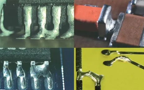
Soldering is one of the most critical steps in PCB assembly. In SMT (Surface Mount Technology), reflow soldering is the standard assembly process. After components are placed, the entire PCB passes through a reflow oven, moving through a series of precisely controlled heating zones that melt the solder paste, allow the molten solder to wet the PCB pads and component terminations, and then solidify into reliable solder joints.
But there's one defect in this process that drives engineers up the wall: solder bridging.
What Is Bridging, and How Serious Is It?
Bridging, also known as solder bridging, is one of the most common defects in SMT assembly. In simple terms, it occurs when excess solder forms an unintended "bridge" between two solder joints that should remain electrically separate, creating an unwanted electrical connection. From a technical standpoint, solder bridging is defined as an unintended electrical connection formed between two or more independent solder joints due to excess solder or uncontrolled solder flow.
In SMT soldering, solder bridging is one of the most common defects. Its consequences go far beyond cosmetic appearance. At best, it can cause circuit malfunctions, signal integrity issues, or intermittent failures. At worst, it can create electrical short circuits that damage the PCB or sensitive electronic components. Even more importantly, solder bridging rarely occurs in isolation. If one solder bridge is detected on a board, it often indicates that the manufacturing process has drifted outside its optimal process window, putting other solder joints at risk as well. Therefore, simply removing the solder bridge isn't enough—you need to identify and eliminate the root cause within the manufacturing process.
So how does solder bridging occur? It generally comes down to four main causes.
1. Poor PCB Design — The Problem Starts on the Drawing BoardMany soldering defects originate long before production begins. Problems introduced during PCB design often become apparent during reflow soldering. Two of the most common design-related causes are poor component placement and insufficient pad spacing.
Poor Component Placement
If a cluster of heavy components is concentrated in one area of the PCB, the board may experience excessive warpage during the reflow process as the substrate softens under high temperatures. Severe PCB warpage can alter the distribution of molten solder during reflow, increasing the risk of solder bridging. Although this is generally a secondary factor compared with solder paste printing or stencil design, it can still contribute to bridging on complex assemblies.
Insufficient Pad Spacing
As electronic products continue to shrink, fine-pitch packages such as QFP (Quad Flat Package) and QFN (Quad Flat No-lead) often feature pad spacing as narrow as 0.4 mm or even 0.3 mm. Without proper Design for Manufacturability (DFM) considerations, even a slight deviation in solder paste printing may cause adjacent solder deposits to merge during reflow.
Prevention Tip
Apply DFM principles during PCB layout. Distribute components evenly to minimize the risk of PCB warpage. For fine-pitch devices, incorporate solder mask dams between adjacent pads whenever possible. This is one of the most effective ways to reduce the risk of solder bridging.
2. Solder Paste Issues — Choosing the Wrong Solder Paste Can Undermine the Entire Process
Solder paste selection and management form the foundation of soldering quality. Even a well-designed PCB and an optimized reflow profile cannot compensate for poor solder paste practices.
Choosing the Wrong Solder Paste
Leaded and lead-free solder pastes have significantly different melting temperatures. For example, Sn63Pb37 solder paste melts at approximately 183°C, while SAC305 lead-free solder paste melts at around 217–220°C. Their recommended preheat profiles, peak temperatures, and process windows differ accordingly. If the selected reflow profile does not match the solder paste, the solder may fail to melt completely or become excessively fluid, increasing the likelihood of solder bridging.
Poor Solder Paste Management
Excessive solder paste volume is one of the most common causes of solder bridging. If too much solder paste is deposited, the molten solder may overflow the available pad area during reflow and spread onto adjacent pads.
Less obvious issues include expired solder paste, which gradually loses flux activity and wetting performance, resulting in unstable solder flow. Fresh and used solder paste should never be mixed, as differences in viscosity and metal content can make printing performance unpredictable.
Prevention Tip
Select solder paste according to your product requirements and process specifications. Store solder paste under recommended refrigerated conditions (typically 2–10°C), allow it to thaw for at least four hours before use, and consume it within the manufacturer's recommended working life after opening. Regularly verify solder paste print thickness and never mix fresh and used solder paste.
3. Improper Reflow Temperature Profiles Lead to Uncontrolled Solder Flow
Reflow soldering is much more than simply heating and cooling the PCB. Every product requires a carefully controlled temperature profile to ensure stable solder wetting and solidification.
A typical reflow profile consists of four stages:
Preheat Zone
The temperature gradually rises from room temperature to approximately 150°C, allowing the PCB and components to heat evenly while volatile solvents within the solder paste evaporate. The recommended heating rate is typically between 1–3°C/s.
Soak Zone
The PCB remains between approximately 150°C and 180°C for 60–120 seconds. During this stage, the flux is fully activated, removing oxides from PCB pads and component terminations to prepare for soldering.
Reflow Zone
The temperature rises to the peak reflow temperature—typically 205–225°C for leaded soldering and 235–250°C for lead-free soldering. The solder paste melts completely and wets the PCB pads and component terminations.
Cooling Zone
The PCB cools at approximately 2–4°C/s, allowing the molten solder to solidify rapidly into strong and reliable solder joints.
Any deviation from the recommended temperature profile can increase the risk of solder bridging. If the preheat ramp is too fast, solvents may not evaporate completely, causing solder paste spattering. If the soak period is too short, the flux may not fully activate, resulting in inconsistent wetting. If the peak temperature is too high or the time above liquidus is too long, the molten solder may exhibit excessive wetting and spreading. If cooling is too slow, the molten solder remains liquid longer, increasing the opportunity for unwanted solder flow.
Prevention Tip
Run a thermal profile for every new product before mass production. Use a thermal profiler to measure actual board temperatures throughout the reflow oven and verify that they remain within the solder paste manufacturer's recommended process window. Re-profile whenever the PCB design, solder paste, or process parameters change.
4. Stencil Issues — Poor Stencil Printing Leads to Soldering Defects
Solder paste printing is the first critical process in SMT assembly, and stencil quality and alignment directly determine print consistency.
Every stencil aperture must align precisely with its corresponding PCB pad. Oversized apertures deposit excessive solder paste, while undersized apertures may cause insufficient solder deposition. Stencil thickness should also match the component package. Fine-pitch components typically require thinner stencils (around 0.10 mm), while larger components may require thicker stencils (0.15–0.20 mm). Complex assemblies sometimes require step stencils with multiple thicknesses.
Mechanical accuracy is equally important. Insufficient stencil tension, poor printer alignment, or stencil deformation can all cause printing misalignment. Another frequently overlooked factor is stencil release. If the stencil separation speed or distance is improperly adjusted, the solder paste may be pulled upward during stencil release, creating peaks or distorted deposits that significantly increase the likelihood of solder bridging.
Prevention Tip
Design stencil apertures in accordance with IPC-7525 guidelines. Regularly verify stencil tension (typically ≥35 N/cm²) and use SPI (Solder Paste Inspection) to monitor solder paste volume, alignment, and print quality during production. Correct abnormalities immediately before they propagate through subsequent manufacturing processes.
Closing Thoughts
Solder bridging may not be the most severe SMT defect, but it is one of the clearest indicators of overall process capability. A manufacturer with a consistently low solder bridging rate typically has well-controlled design reviews, material management, process control, equipment maintenance, and quality assurance procedures. Conversely, if solder bridging occurs frequently, the problem rarely lies in a single process step—the entire manufacturing system should be reviewed.
Based on practical manufacturing experience, an effective troubleshooting sequence for solder bridging is as follows: first, verify stencil printing quality and alignment, since these are usually the quickest variables to confirm. Next, inspect the solder paste to ensure it is fresh, properly stored, and correctly prepared. Then review the reflow temperature profile to confirm it remains within specification. Finally, evaluate the PCB design, including pad spacing, component placement, and solder mask dam design.
Never take a solder joint for granted. A properly soldered PCB can operate reliably for more than a decade, while a poorly soldered one may fail before it even leaves the factory. Process engineering is all about attention to detail. Solder bridging may be a long-standing challenge in SMT manufacturing, but with rigorous design, material control, and process optimization, it is entirely preventable.