

SMT Assembly Process: A Complete Guide to Surface Mount Technology in PCB Manufacturing
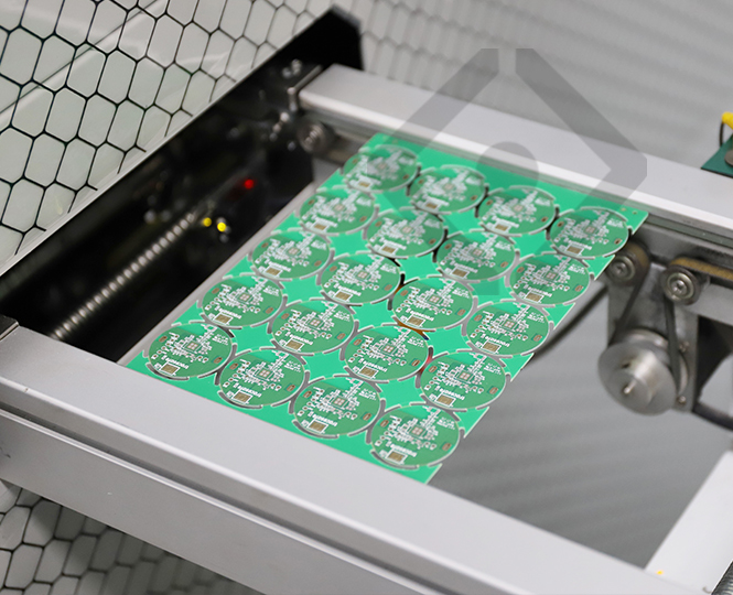
Surface Mount Technology (SMT) is a core process in modern PCB assembly. Unlike traditional Through-Hole Technology (THT), which requires component leads to be inserted into drilled holes on a PCB, SMT mounts electronic components directly onto the surface of a printed circuit board.
By enabling high-density component placement, improved production efficiency, and reliable electrical performance, SMT has become the dominant assembly method in modern electronics manufacturing. The following sections introduce the standard SMT assembly process and its key manufacturing steps.
1. PCB, Component, and Stencil Preparation
Before SMT assembly begins, proper preparation of the PCB, electronic components, and stencil is essential.
Depending on storage conditions and component requirements, PCBs and moisture-sensitive components may undergo cleaning or baking processes to remove surface contaminants and reduce moisture-related risks that could affect soldering quality.
At the same time, the SMT stencil is designed and manufactured according to PCB layout data to ensure accurate aperture positioning for solder paste printing.
Proper preparation at this stage provides a solid foundation for stable and consistent SMT assembly.
2. Solder Paste Printing
Solder paste printing is the first major step in the SMT assembly process.
Solder paste, which consists of solder alloy powder and flux, acts as the bonding material between electronic components and PCB pads. Using an automated solder paste printer, the paste is accurately deposited onto the PCB surface through a precision stencil, creating solder paste patterns on designated pads.
The accuracy of solder paste printing is critical, as paste volume, thickness, and alignment directly affect the quality and reliability of final solder joints.
In high-quality SMT manufacturing, Solder Paste Inspection (SPI) may be used after printing to verify solder paste volume, height, and positioning, helping identify potential printing issues before component placement.
3. Component Placement
After solder paste printing, the PCB enters the component placement stage.
An automated pick-and-place machine precisely places surface mount components, including resistors, capacitors, ICs, connectors, and other electronic devices, onto their designated PCB pads according to programmed assembly data.
The machine retrieves components from tape-and-reel, tray, or tube packaging and places them onto the PCB at high speed with micron-level accuracy.
Accurate component positioning and orientation are essential to ensure proper alignment before soldering and achieve reliable assembly quality.
4. Reflow Soldering
After component placement, the PCB proceeds to the reflow soldering stage.
Reflow soldering is the primary soldering method used in SMT assembly. During this process, the PCB passes through a reflow oven with multiple temperature zones. The controlled heating process allows the solder paste to gradually melt, allowing the solder alloy to wet the PCB pads and component terminals before cooling and solidifying into reliable solder joints.
A typical reflow soldering process includes four stages:
Preheating Zone
The PCB temperature gradually increases, allowing the PCB, components, and solder paste to heat evenly. This reduces thermal stress and prevents component damage caused by rapid temperature changes.
Soaking Zone
The flux becomes activated, helping remove oxidation effects from metal surfaces and improving solder wettability between the solder paste, PCB pads, and component terminals.
Reflow Zone
The temperature rises above the melting point of the solder alloy, causing the solder particles to melt and form reliable mechanical and electrical connections between components and PCB pads.
Cooling Zone
The molten solder gradually solidifies under controlled cooling conditions, forming stable solder joints with good mechanical strength and electrical performance.
5. Inspection and Rework
After soldering is completed, assembled PCBs may undergo inspection and rework processes to ensure manufacturing quality.
Common inspection methods include Automated Optical Inspection (AOI), which detects component placement and visible solder defects, and X-ray inspection, which is used for inspecting hidden solder joints such as those under BGA and other area-array packages.
If defects are identified, rework procedures are performed to correct issues and ensure the assembled PCB meets quality requirements.
Conclusion
SMT assembly is a fundamental technology in modern PCB manufacturing. Through a precisely controlled sequence of preparation, solder paste printing, component placement, reflow soldering, and quality control, SMT enables efficient, high-density, and reliable circuit board production.
For PCB assembly manufacturers, mastering every stage of the SMT process — from stencil design and solder paste printing to component placement and reflow soldering — is essential to delivering consistent product quality and meeting the increasingly demanding requirements of the electronics industry.
With advanced manufacturing equipment, optimized process control, and strict quality management, professional SMT assembly providers can ensure reliable PCB performance and long-term product stability.