

What Causes SMT Tombstoning?
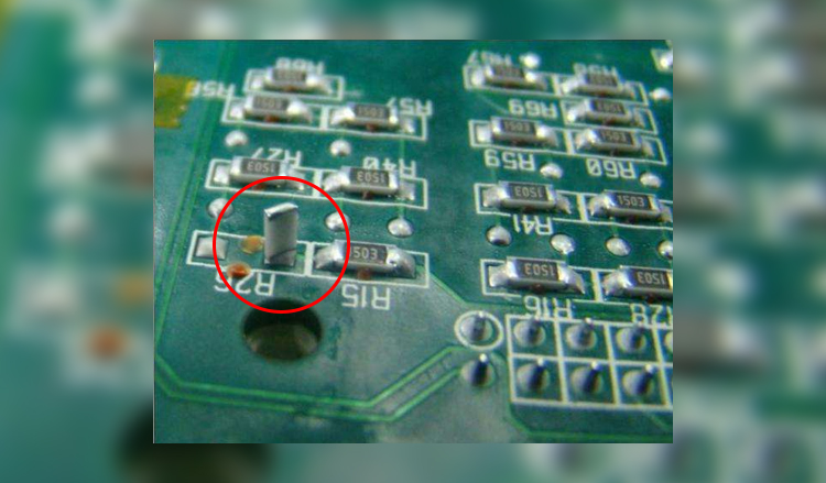
Tombstoning mainly occurs during the SMT reflow soldering process. It happens when one end of a component lifts away from the PCB pad while the other end remains soldered to the board, leaving the component standing vertically or at an angle. Because the component may resemble a tombstone standing on one end, this defect is commonly known as the tombstone effect. It is also sometimes referred to as the Manhattan effect.
What Is the SMT Tombstone Effect?
The tombstone effect occurs when the solder on the two ends of a component melts and wets the corresponding pads at different times or with different forces.
When solder paste melts during reflow, surface tension develops between the molten solder and the component terminals. Ideally, both ends of the component should experience similar wetting conditions and surface tension, allowing the component to remain properly positioned on the PCB.
However, if one side wets earlier or contains more solder than the other side, the surface tension on the two ends becomes unbalanced. The stronger pulling force can lift one end of the component away from the PCB, producing the tombstone effect.
Once one end is lifted, a complete solder joint cannot be formed on that side, which may result in an open circuit or an electrical connection failure.
What Causes SMT Tombstoning?
Tombstoning is usually caused by an imbalance in solder wetting and surface tension between the two ends of a component. Several factors can contribute to this imbalance.
1. Uneven Heating During Reflow
Uneven heating is one of the important factors that can contribute to tombstoning.
During reflow soldering, the PCB assembly passes through a controlled thermal profile consisting of stages such as preheating, soaking, reflow, and cooling. If one area of the PCB heats significantly faster than another, the solder paste on one pad may melt and begin wetting earlier.
When one end of a component becomes soldered before the other end, the surface tension generated at that end may pull the component upward before the second solder joint has properly formed.
An improperly optimized reflow profile, excessive heating rate, or significant thermal differences across the PCB can therefore increase the risk of tombstoning.
2. Unequal Solder Paste Volume
Unequal solder paste deposits on the two pads are another common cause of tombstoning.
If one pad receives significantly more solder paste than the other, the amount of molten solder and the resulting surface tension can differ between the two ends of the component.
During reflow, the side with the larger or earlier-melting solder deposit may exert a stronger pulling force, causing the component to rotate or lift.
Accurate stencil design, consistent solder paste printing, and proper control of solder paste volume are therefore important for preventing tombstoning.
3. Improper Pad Design
PCB pad geometry has a direct influence on solder wetting and component positioning.
If the two pads are not properly matched in size, shape, spacing, or solderability, the solder may wet one side differently from the other. This can create an imbalance in surface tension during reflow.
For small chip components, the pad dimensions and spacing should follow the relevant component manufacturer's recommendations and appropriate PCB design guidelines.
4. Component Placement Offset
Incorrect component placement can also increase the risk of tombstoning.
If a component is significantly offset from the centerline of its two pads, the solder deposits and component terminals may not be properly aligned. During reflow, this can contribute to uneven wetting forces and cause the component to move or rotate.
Maintaining accurate pick-and-place positioning is particularly important for small passive components with narrow pad spacing.
5. Differences in Pad or Component Solderability
The solderability of the PCB pads and component terminals can also affect tombstoning.
Oxidation, contamination, poor surface finish condition, or differences in the solderability of the two pads can cause one side of the component to wet more quickly than the other.
When the solder on one side melts and wets the terminal earlier, an imbalance in surface tension may develop and lift the opposite end of the component.
Proper material storage and handling are therefore important for maintaining good solderability.
6. Component Size and Geometry
Very small and lightweight passive components are generally more susceptible to tombstoning because the surface-tension forces generated during soldering can have a greater effect on them.
However, component size alone does not cause tombstoning. The defect usually occurs when component geometry interacts with other factors, such as uneven solder paste deposits, pad design, placement offset, and differences in wetting.
7. Stencil Design and Printing Parameters
Stencil thickness, aperture design, printing alignment, squeegee pressure, and printing speed can all affect solder paste deposition.
If the two pads of a component receive different amounts of solder paste, the resulting imbalance can increase the likelihood of tombstoning.
For fine-pitch and small passive components, the stencil aperture design should therefore be carefully optimized to achieve consistent solder paste volume on both pads.
How to Prevent SMT Tombstoning?
Preventing tombstoning requires control of the entire SMT assembly process rather than relying on a single adjustment.
1. Optimize the Reflow Temperature Profile
The reflow temperature profile should be properly established according to the solder paste manufacturer's recommendations, PCB design, and component requirements.
The heating rate, soak conditions, peak temperature, time above liquidus, and cooling rate should be appropriately controlled to promote balanced and consistent solder wetting.
2. Ensure Consistent Solder Paste Printing
Solder paste should be deposited evenly on both pads of each component.
The stencil thickness and aperture dimensions should be designed according to the component package and PCB pad geometry. The solder paste printer should also be properly calibrated to maintain accurate alignment and consistent deposition.
3. Optimize PCB Pad Design
The two pads of a component should have appropriate dimensions, spacing, and symmetry.
Proper pad design helps ensure that solder paste is deposited consistently and that both ends of the component experience similar soldering conditions during reflow.
4. Improve Component Placement Accuracy
The pick-and-place machine should be regularly maintained and calibrated to ensure accurate component positioning.
Correct placement helps keep the component centered between the two pads and reduces the possibility of uneven solder wetting.
5. Control PCB and Component Cleanliness
PCB pads and component terminals should be properly protected from oxidation and contamination.
Proper storage, handling, and material management can help maintain consistent solderability and reduce differences in wetting between the two ends of a component.
6. Optimize Stencil and Printing Parameters
For components that are particularly susceptible to tombstoning, the stencil aperture design and printing parameters may need to be optimized to achieve more balanced solder paste deposits.
Parameters such as stencil thickness, aperture geometry, printing speed, and squeegee pressure should be selected according to the PCB design and solder paste characteristics.
Conclusion
SMT tombstoning is a common reflow soldering defect in which one end of a surface-mount component lifts away from the PCB pad while the other end remains soldered. The primary mechanism is an imbalance in solder melting and wetting between the two ends of the component, which creates unequal surface-tension forces.
Common contributing factors include uneven heating, unequal solder paste volume, improper PCB pad design, component placement offset, differences in solderability, and unsuitable stencil or printing parameters.
To reduce tombstoning, PCB assembly manufacturers should focus on balanced solder paste deposition, proper pad design, accurate component placement, stable material conditions, and a well-controlled reflow temperature profile. These measures help ensure that both ends of the component are soldered under similar conditions, improving assembly consistency and reducing the risk of open solder joints.