

Why Does Component Offset Occur During SMT Assembly?
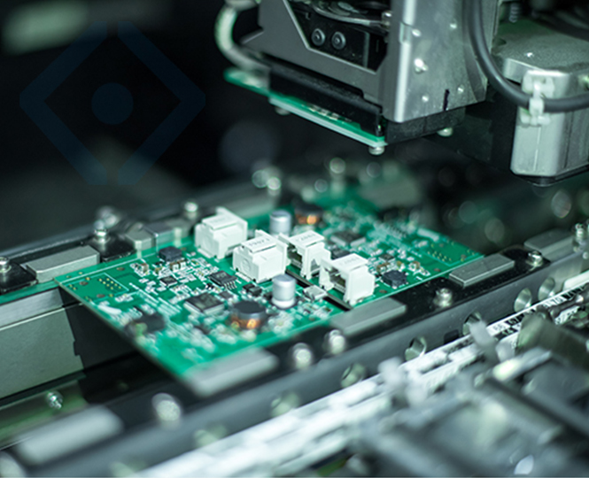
Component offset is a common issue that can occur during the PCB assembly process, particularly during SMT component placement and reflow soldering. If components are not positioned correctly on the PCB pads, the resulting solder joints may be uneven or incomplete, potentially affecting the electrical and mechanical reliability of the PCBA.
Component offset can occur before reflow, during component placement, or after the solder paste melts during reflow. Therefore, identifying the actual cause is important for determining the appropriate corrective action.
What Is Component Offset in PCB Assembly?
Component offset refers to a situation in which an electronic component is not positioned correctly relative to its intended PCB pads.
During SMT assembly, a pick-and-place machine places components onto solder paste deposits on the PCB. Ideally, the component terminals should be properly aligned with the corresponding pads.
A small amount of self-alignment can occur during reflow because the surface tension of molten solder tends to pull the component toward a more stable position. However, excessive initial placement errors or significant differences in solder paste deposition can prevent proper alignment. Component offset may appear as horizontal displacement, rotation, or uneven positioning between the component and its pads.
Causes of Component Offset During PCB Assembly
Several factors can contribute to component offset during SMT assembly.
1. Solder Paste Printing Misalignment
Solder paste printing is one of the most important factors affecting component positioning.
If the stencil is not correctly aligned with the PCB, solder paste may be deposited away from the center of the intended pads. When the component is placed onto these deposits, it may also be positioned incorrectly.
Uneven solder paste volume between two pads can be particularly problematic for small passive components. During reflow, the difference in molten solder volume and wetting force may cause the component to move or rotate.
Therefore, accurate stencil alignment and consistent solder paste deposition are essential.
2. Pick-and-Place Machine Accuracy
The pick-and-place machine is responsible for accurately positioning components on the PCB. If the machine is not properly calibrated or maintained, placement errors may occur.
Possible causes include incorrect placement coordinates, machine calibration errors, worn mechanical components, inaccurate vision recognition, or improper feeder settings.
For high-density SMT assemblies, even a small placement error can become significant, particularly when working with fine-pitch components.
Regular equipment calibration and maintenance can help maintain placement accuracy.
3. PCB Positioning and Fiducial Issues
The PCB must be accurately positioned before component placement.
SMT machines typically use fiducial marks and vision systems to determine the PCB's actual position and orientation. If fiducial marks are poorly designed, damaged, contaminated, or incorrectly defined in the assembly program, the machine may calculate the PCB position inaccurately.
This can cause multiple components to be offset in a similar direction.
Proper fiducial design, PCB positioning, and accurate assembly programming are therefore important for maintaining placement accuracy.
4. Component Pickup Problems
Problems during component pickup can also result in incorrect placement.
For example, if the nozzle does not pick up a component correctly, the component may be tilted, shifted, or incorrectly oriented before placement. Feeder problems, unsuitable nozzle selection, component packaging issues, or contamination on the nozzle can also affect component pickup.
If the component is not properly centered on the nozzle, its final placement position may deviate from the programmed coordinates.
5. Improper PCB Pad Design
PCB pad design can influence component positioning and solder joint formation.
If pad dimensions, spacing, or symmetry are inappropriate for the selected component package, the component may not sit properly on the solder paste deposits.
For small chip components, asymmetric pads or significantly different solder paste volumes between the two sides can increase the risk of component movement or rotation during reflow.
PCB footprints should therefore be designed according to the component manufacturer's recommended land patterns and applicable design standards.
6. Uneven Solder Paste Volume
Even when the stencil is correctly aligned, inconsistent solder paste volume can cause component movement during reflow.
If one pad receives significantly more solder paste than the other, the two sides of the component may experience different wetting forces when the solder melts.
This is particularly important for two-terminal components such as chip resistors and capacitors, where an imbalance in solder volume can contribute to component rotation or tombstoning.
7. Reflow Temperature Profile
Component offset can also occur during reflow soldering.
As the solder paste melts, molten solder generates surface tension between the component terminals and PCB pads. Under normal conditions, these forces can help center the component.
However, if the two sides of the component do not melt or wet at approximately the same time, the resulting surface-tension forces may become unbalanced. The component can then move, rotate, or, in more severe cases, develop a tombstone defect.
An improperly optimized reflow profile can therefore contribute to component movement after placement.
8. PCB or Material Contamination
Contamination on PCB pads or component terminals can affect solder wetting.
Oxidation, dust, oil, or other contaminants may cause one pad to wet differently from another. This can create uneven soldering forces during reflow and potentially result in component movement.
Proper storage, handling, and cleanliness control of PCBs and electronic components are therefore important.
How to Reduce Component Offset During PCB Assembly
Reducing component offset requires coordinated control of the SMT process rather than relying on a single adjustment.
1. Improve Solder Paste Printing Accuracy
The stencil should be properly aligned with the PCB, and its thickness and aperture design should match the PCB pad geometry and component package.
Printing parameters such as printing speed, squeegee pressure, and stencil condition should also be controlled to maintain consistent solder paste deposits.
For high-density assemblies, solder paste inspection can be used to monitor deposit volume, height, area, and position.
2. Maintain and Calibrate Pick-and-Place Equipment
Pick-and-place machines should be regularly maintained and calibrated.
The vision system, placement coordinates, feeders, nozzles, and mechanical positioning system should be checked to ensure accurate component pickup and placement.
If multiple components show a similar offset pattern, equipment calibration or PCB positioning should be investigated.
3. Optimize PCB Fiducial Design
Appropriate fiducial marks should be included in the PCB design when required by the assembly process.
Fiducials provide reference points for the pick-and-place machine's vision system and help compensate for PCB positioning and rotation errors.
4. Use Appropriate Component Footprints
PCB footprints should follow the component manufacturer's recommended land patterns whenever possible.
Pad size, spacing, symmetry, and solder mask design should be considered together to ensure that components can be accurately placed and reliably soldered.
5. Control Solder Paste Volume
Solder paste volume should be balanced between corresponding pads.
Proper stencil design and stable printing conditions can help prevent excessive differences in solder paste deposition. This is especially important for fine-pitch components and small passive devices.
6. Optimize the Reflow Profile
The reflow temperature profile should be established according to the solder paste manufacturer's recommendations and the PCB assembly requirements.
Proper control of the heating rate, soak stage, peak temperature, time above liquidus, and cooling rate helps ensure consistent solder melting and wetting.
A stable thermal profile can reduce unnecessary component movement during reflow.
7. Improve Material Storage and Handling
PCBs and electronic components should be stored and handled according to their respective requirements.
Materials should be protected from moisture, oxidation, dust, and other contaminants that could affect solderability and assembly quality.
Conclusion
Component offset during PCB assembly can occur during both the SMT placement stage and the subsequent reflow soldering process. Common causes include solder paste printing misalignment, inconsistent solder paste volume, pick-and-place errors, PCB positioning problems, component pickup issues, improper PCB footprints, and unbalanced solder wetting during reflow.
To reduce component offset, PCB assembly manufacturers should maintain accurate solder paste printing, properly calibrate pick-and-place equipment, use appropriate PCB footprints and fiducial marks, control material conditions, and optimize the reflow temperature profile.
Effective control of these factors helps improve component placement accuracy, solder joint consistency, and the overall reliability of PCBA products.