

What Is a PCB Pad? Types, Manufacturing, and Common Defects
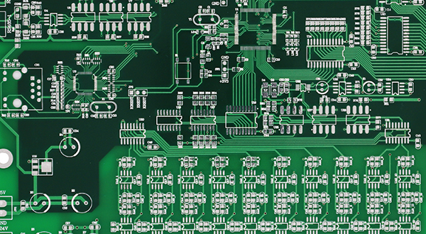
A PCB pad is a designated conductive area on a printed circuit board used to connect a component terminal or provide a contact point. Most component solder pads consist of copper protected by a solderable surface finish. During PCB assembly, solder forms an electrical and mechanical connection between the pad and the component.Pad geometry, surface condition, and placement influence solder joint formation. Understanding these features helps engineers design manufacturable boards and diagnose assembly defects.
What Does a PCB Pad Do?
Component solder pads connect component leads, terminals, or solder balls to the board’s circuitry. Some also provide a path for heat transfer, particularly beneath power devices and packages with exposed thermal pads.
The arrangement of pads for a component forms its land pattern, which is part of the PCB footprint. Pad dimensions should account for the component package, manufacturing tolerances, and assembly process rather than simply matching the terminal dimensions.
Not every PCB pad is intended for soldering. Test pads, for example, provide access for electrical probes during inspection or testing.
Main Types of PCB Solder Pads
Surface-Mount Pads
Surface-mount pads connect components directly to the board surface without requiring their terminals to pass through component holes. During SMT assembly, solder paste is typically printed onto these pads before component placement and reflow soldering.
Common shapes include rectangles, rounded rectangles, and circles. The appropriate geometry depends on the package: chip components commonly use rectangular pads, while ball grid array (BGA) packages typically use circular pads.
Surface-mount technology supports compact layouts, but pad type alone does not determine reliability or electromagnetic performance. Those outcomes also depend on circuit layout, grounding, materials, and assembly quality.
Through-Hole Pads
Through-hole pads surround holes that receive component leads. On a typical plated-through-hole PCB, the copper pad around the hole is connected to a plated copper barrel along the hole wall. Solder joins the inserted lead to these conductive surfaces.
The copper surrounding the hole is called the annular ring. Its dimensions, together with the finished hole size and fabrication tolerances, are important to connection integrity.
Through-hole mounting can provide useful mechanical support for connectors and other mechanically loaded components. However, it does not automatically provide greater current capacity than surface mounting. Current capacity depends on the complete conductive path, including the lead, copper thickness, barrel plating, connected traces or planes, and allowable temperature rise.
Thermal Pads
Some packages require a larger PCB pad beneath the component’s exposed pad to transfer heat into the board. This pad may also require an electrical connection, such as ground, according to the component datasheet.
Its copper layout, thermal vias, and solder paste pattern should follow the device manufacturer’s recommendations. Texas Instruments’ QFN and SON attachment guide
How Solder Mask Affects Pad Design
Solder mask covers selected areas of the PCB while leaving openings for soldering. Two common pad configurations are:
Non-solder-mask-defined (NSMD): The mask opening is larger than the copper pad, so the copper geometry defines the pad boundary.
Solder-mask-defined (SMD): The mask overlaps the copper perimeter, so the opening defines the exposed solderable area.
Here, SMD means “solder-mask-defined,� not “surface-mount device.� The appropriate configuration depends on the package and fabrication requirements; neither should be selected as a universal rule. Texas Instruments’ pad design guidance
Where manufacturing clearances permit, solder mask webs between neighboring pads help limit solder bridging. They do not compensate for excessive solder paste or inaccurate printing. Eurocircuits solder mask guidelines
How Are PCB Pads Manufactured?
PCB pads are formed as part of the board’s copper circuitry. Manufacturers do not normally apply separate pieces of copper foil only at pad locations.
A conventional fabrication process uses copper-clad laminate, imaging, etching, and—where required—copper plating to produce pads and traces. Through-holes are drilled and metallized when electrical connections through the board are required. The exact sequence varies with the board construction and fabrication method.
Solder mask is then patterned to expose the intended connection areas. A surface finish protects exposed copper and preserves solderability. Common options include:
HASL: Hot air solder leveling leaves a solder coating on exposed copper.
ENIG: Electroless nickel immersion gold forms a nickel layer with a thin immersion gold coating.
OSP: Organic solderability preservative uses an organic protective coating rather than a metallic finish.
Finish selection should consider pad geometry, assembly requirements, storage conditions, and cost. Inspection and electrical testing help identify fabrication defects before assembly. Eurocircuits PCB manufacturing overview
Common Pad and Solder Joint Problems
A defect near a pad may originate in PCB fabrication, footprint design, or assembly. Identifying the source is more useful than changing soldering temperature alone.
Solder Bridges and Shorts
A solder bridge unintentionally connects adjacent conductors. Possible contributors include excess solder paste, printing misalignment, inadequate spacing, and unsuitable stencil apertures.
Check the footprint, solder mask openings, paste deposits, and placement accuracy. A bare-board short caused by unwanted copper requires a different investigation from an assembly-related solder bridge.
Open Connections and Poor Wetting
An open connection can result from insufficient solder, contamination, oxidation, component misalignment, or an unsuitable thermal profile. Damaged pads or broken traces can also interrupt the circuit.
Inspect the board and component surfaces, verify paste deposition and placement, and measure the actual thermal profile. Increasing temperature without identifying the cause can damage components or the PCB.
Solder Joint Voids
Voids are cavities within the solder joint, rather than necessarily defects in the copper pad. They can form when gases become trapped during soldering.
For exposed-pad packages, review paste selection, stencil aperture design, via configuration, and reflow conditions. X-ray inspection can reveal voids hidden beneath components. Texas Instruments’ assembly and inspection guidance
Void acceptability depends on the package, application, and applicable requirements. A single universal limit is inappropriate.
Lifted or Damaged Pads
Pads may separate from the laminate because of excessive heating, repeated rework, mechanical force, or inadequate copper adhesion.
Use a controlled rework process and avoid pulling components before the solder has fully melted. Evaluate damaged pads against the applicable repair and acceptance requirements before returning the assembly to service.
What Should Engineers Check Before Production?
Start with the component manufacturer’s recommended land pattern, then confirm that it is compatible with the PCB supplier’s capabilities and the assembly process.
Review pad spacing, hole sizes, annular rings, solder mask clearances, surface finish, and solder paste apertures together. Coordinating these details before production helps prevent defects that cannot be resolved through soldering adjustments alone.