

PCB X-Ray Inspection: Methods, Defects, and Limitations
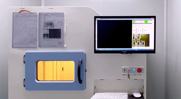
PCB X-ray inspection uses penetrating electromagnetic radiation to examine solder joints and internal features that are difficult or impossible to see from the board surface. In printed circuit board assembly (PCBA), it is particularly useful for inspecting connections beneath components such as ball grid arrays (BGAs) and quad flat no-lead (QFN) packages. X-ray inspection helps manufacturers identify hidden assembly defects and investigate process problems. It complements optical inspection and electrical testing, but it cannot independently verify every aspect of product quality or reliability.
Why Is X-Ray Inspection Used in SMT Assembly?
During surface-mount technology (SMT) assembly, components are placed onto solder paste and typically joined to the PCB through reflow soldering.
Automated optical inspection (AOI) can examine visible features such as component position and exposed solder joints. However, component bodies can obscure the connections underneath them. X-ray imaging provides access to these hidden areas without removing the component.
Typical inspection targets include BGA solder balls, solder beneath bottom-terminated components, and selected through-hole connections. Comet Yxlon’s electronics inspection overview
How Does PCB X-Ray Inspection Work?
An X-ray source directs radiation through the assembly toward a detector. Different materials attenuate, or reduce, the transmitted radiation by different amounts.
Image contrast depends on material composition, density, thickness, and X-ray energy. Solder and other metallic features generally attenuate more radiation than the surrounding organic board materials, allowing their shapes and internal variations to become visible.
The detector records a projection of the features along the beam path. Software displays and analyzes this information, or combines multiple projections to reconstruct internal sections.
Conventional electronics X-ray inspection is therefore primarily based on transmission imaging. Describing reflected X-rays from the PCB surface as a standard method for examining internal board connections is inaccurate.
Main X-Ray Inspection Methods
2D X-Ray Imaging
A 2D image combines features at different depths into a single projection. It can reveal solder bridges, missing solder balls, and voids where image contrast and viewing geometry are suitable.
Oblique viewing angles can help distinguish features that overlap in a straight-down image. Nevertheless, dense assemblies and double-sided boards can produce overlapping structures that complicate interpretation. Comet Yxlon’s explanation of 2D inspection limitations
Computed Tomography and Computed Laminography
Computed tomography (CT) reconstructs a three-dimensional representation from multiple X-ray projections. Operators can examine virtual sections through a component or connection.
Computed laminography uses acquisition geometry suited to flat objects such as PCBs. It helps separate features at different depths, making hidden joints easier to evaluate when structures on the opposite side of the board would otherwise overlap them. Comet Yxlon’s computed laminography overview
Reconstruction can provide more detail than a single projection, but inspection time, accessible resolution, and image quality depend on the equipment, scan settings, and assembly.
Manual Inspection and Automated X-Ray Inspection
Manual and automated inspection describe how the equipment is operated, rather than separate imaging principles.
Operator-controlled systems support targeted investigation, process development, and failure analysis. Automated X-ray inspection (AXI) uses programmed acquisition and analysis to evaluate defined inspection locations, including in production lines. Available defect detection functions vary by system and inspection program. Nordson AXI system overview
What Defects Can X-Ray Inspection Detect?
Depending on resolution, viewing angle, and analysis capability, X-ray inspection can help identify:
Solder bridges: Unintended solder connections between adjacent conductors.
Missing or abnormal solder deposits: Missing BGA balls or solder shapes that differ from the expected geometry.
Solder voids: Cavities within solder joints, including beneath exposed thermal pads.
Certain open-joint conditions: Visible separation or abnormal joint geometry.
Through-hole solder fill issues: Incomplete filling of plated holes where the imaging method provides sufficient visibility.
Advanced systems may also help identify head-in-pillow defects, where a BGA ball and solder paste deposit fail to form a proper joint. Such defects are not reliably excluded by a simple top-down image alone. Nordson’s advanced solder joint inspection capabilities
Detection capability should be validated for the actual package, defect type, and production setup.
How Should X-Ray Results Be Evaluated?
Apply Product-Specific Acceptance Criteria
An unusual image does not automatically indicate a rejectable defect. Results should be assessed against the applicable customer requirements, component guidance, and assembly acceptance criteria.
For void analysis, distinguish between projected void area in a 2D image and void volume in a reconstructed dataset. These measurements are not interchangeable. A single void percentage should not be treated as a universal acceptance limit for every package and application.
Combine Imaging with Other Tests
X-ray images show structural information; they do not directly prove electrical continuity, mechanical strength, or long-term reliability.
Some cracks, poorly wetted interfaces, or other defects may be difficult to distinguish at the available resolution. AOI, in-circuit testing, functional testing, and targeted failure analysis provide additional evidence where required.
Practical Limitations and Safety Considerations
X-ray inspection involves equipment investment, programming, interpretation, and maintenance. Throughput depends on the inspected area, number of views, resolution, and reconstruction requirements. A rapid whole-board scan does not necessarily provide detailed coverage of every connection.
Industrial cabinet systems use shielding and safety interlocks to control exposure to ionizing radiation. Operators should follow the equipment manufacturer’s procedures and applicable local requirements. The FDA identifies warning indicators and interlocks among the protective features required for cabinet X-ray systems in the United States. FDA cabinet X-ray system guidance
Where Does X-Ray Inspection Fit in PCBA Quality Control?
X-ray inspection is especially valuable when critical solder connections are hidden from optical inspection. Depending on product risk and customer requirements, manufacturers may use it for process qualification, sampling, targeted troubleshooting, or production inspection.
Its greatest value comes from connecting inspection findings to corrective action in printing, placement, reflow, or board design. Combined with suitable process controls and electrical testing, it helps reduce the risk of hidden defects reaching the finished product.