

What Is PCB Immersion Gold? ENIG Process, Advantages & Applications
What Is the PCB Immersion Gold Process?
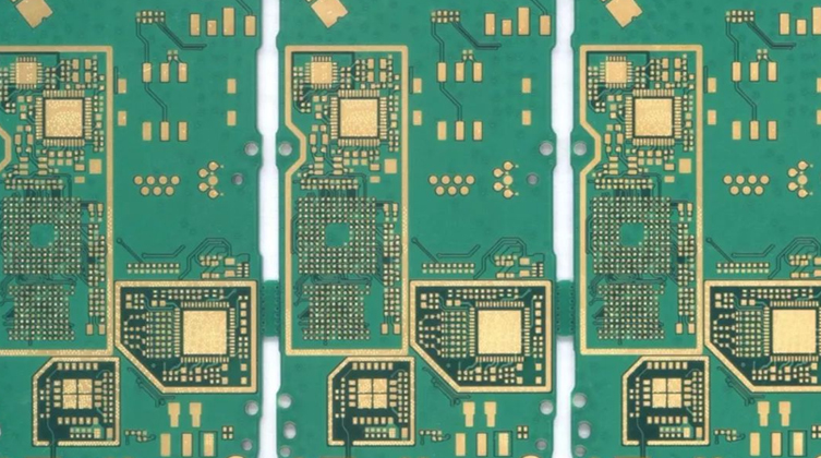
Immersion gold is a widely used surface finish for printed circuit boards (PCBs), particularly for boards that require a flat soldering surface, good solderability, and reliable protection of exposed copper pads.
The most common immersion gold finish used in PCB manufacturing is ENIG (Electroless Nickel Immersion Gold). As the name suggests, the process consists of two main metallic layers: an electroless nickel layer deposited onto the exposed copper surface, followed by a thin immersion gold layer deposited over the nickel.
Unlike electroplated gold, immersion gold does not require an external electrical current to deposit the gold layer. Instead, the gold is deposited through a chemical displacement reaction on the underlying nickel surface.
ENIG is widely used in high-density PCB applications because it provides a relatively flat surface and good solderability while protecting the underlying copper from oxidation.
What Is Immersion Gold on a PCB?
Immersion gold is a PCB surface finish in which a thin layer of gold is chemically deposited over an electroless nickel layer.
The typical ENIG structure can be represented as:
Copper → Electroless Nickel → Immersion Gold
The copper forms the underlying PCB conductor and solder pad. The electroless nickel layer acts as a barrier and provides the surface onto which the immersion gold is deposited. The thin gold layer protects the nickel surface and maintains good solderability before assembly.
Because the gold layer is very thin compared with the nickel layer, ENIG is different from a conventional electroplated gold finish, which is generally designed for applications requiring a thicker and more wear-resistant gold coating.
How Does the ENIG Process Work?
The ENIG process involves a series of controlled chemical treatments. The exact sequence can vary depending on the PCB manufacturer's chemistry and process line, but the general process includes the following stages.
1. Copper Surface Cleaning
The exposed copper areas are first cleaned to remove oil, organic contamination, oxides, and other residues.
A clean copper surface is essential because contamination can interfere with subsequent activation and electroless nickel deposition.
2. Micro-Etching
The copper surface is typically micro-etched to remove a controlled amount of copper and prepare the surface for subsequent chemical treatment.
Micro-etching helps remove surface oxides and contaminants while providing a suitable surface condition for the electroless nickel process.
The amount of copper removed must be carefully controlled because excessive micro-etching can affect the PCB pad geometry.
3. Activation
The cleaned copper surface is activated so that electroless nickel deposition can begin.
In a conventional ENIG process, a catalytic activation system based on palladium is commonly used. The catalyst provides the active sites required for the subsequent electroless nickel deposition.
4. Electroless Nickel Plating
After activation, the PCB enters the electroless nickel bath.
Unlike electroplating, electroless nickel deposition does not rely on an external electrical current. Instead, a chemical reduction reaction deposits nickel onto the activated copper surface.
The resulting nickel layer serves several important functions. It provides a suitable surface for the immersion gold layer, acts as a barrier between the copper and gold, and contributes to the mechanical and soldering properties of the finished surface.
5. Immersion Gold Deposition
After the nickel layer has been formed, the PCB is transferred to the immersion gold bath.
Gold is deposited onto the nickel surface through a controlled displacement reaction. In this reaction, nickel at the surface is displaced while gold is deposited onto the exposed nickel.
The resulting gold layer is thin and uniform and protects the nickel surface from oxidation and contamination before PCB assembly.
The gold layer also provides a suitable surface for soldering during SMT or other assembly processes.
6. Rinsing and Drying
After the chemical treatments, the PCB is thoroughly rinsed and dried according to the process requirements.
Proper rinsing is important for removing residual chemicals and preventing contamination between process stages.
Advantages of ENIG Surface Finish
ENIG has become a popular PCB surface finish because it combines a relatively flat surface with good solderability and copper protection.
Flat Surface for Fine-Pitch Components
One of the major advantages of ENIG is its relatively flat surface.
Unlike HASL, which can produce variations in solder coating thickness and pad height, ENIG provides a more uniform surface. This makes it well suited to fine-pitch components, BGA packages, and high-density SMT assemblies.
A flat surface is particularly important when accurate solder paste printing and consistent component placement are required.
Good Solderability
ENIG provides a suitable surface for soldering and is widely used in SMT assembly.
The gold layer protects the underlying nickel before assembly, while the soldering process allows the solder to form a connection with the underlying metallic structure.
Proper control of the ENIG process is important because surface condition and nickel/gold layer quality can directly affect soldering performance.
Good Oxidation Protection
The immersion gold layer protects the nickel surface from oxidation during storage and handling.
This helps maintain the solderability of PCB pads before the boards are assembled.
However, ENIG should not be regarded as an unlimited corrosion barrier. Proper PCB packaging and storage remain important, particularly for boards that will be stored for extended periods.
Suitable for High-Density PCB Designs
Because ENIG provides a relatively flat and uniform surface, it is suitable for many high-density PCB designs.
It can be used with fine-pitch components and area-array packages such as BGAs, making it a common choice for complex electronic assemblies.
Suitable for Multiple Assembly Requirements
ENIG can be used in many PCB assembly processes and is commonly selected for products requiring a consistent soldering surface.
Its suitability for reflow soldering and other assembly processes makes it useful across a wide range of electronic applications.
Limitations of ENIG
Although ENIG offers several advantages, it also has limitations that should be considered during PCB design and manufacturing.
Higher Cost Than Some Surface Finishes
ENIG generally costs more than some simpler PCB surface finishes, such as OSP or HASL.
The additional chemical processing and metallic layers contribute to the overall manufacturing cost. Therefore, ENIG should be selected when its technical benefits justify the additional cost.
Nickel Layer Quality Is Important
The quality of the electroless nickel layer is critical to ENIG performance.
Poor process control can lead to defects such as uneven deposition or other surface-related problems. In severe cases, issues associated with the nickel surface can affect solder joint reliability.
Therefore, ENIG chemistry, bath conditions, surface preparation, and process control must be carefully managed during PCB manufacturing.
Not the Same as Hard Gold
ENIG should not be confused with hard gold plating.
The immersion gold layer is relatively thin and is primarily intended to protect the nickel surface and maintain solderability. It is not designed to withstand the repeated mechanical wear associated with connector contacts.
For edge connectors, key switches, or other applications involving repeated physical contact, a suitable hard gold finish may be required instead.
ENIG vs. Other PCB Surface Finishes
Different PCB surface finishes are designed for different applications.
ENIG vs. OSP
OSP uses an organic protective coating over exposed copper, while ENIG uses electroless nickel and immersion gold.
OSP generally provides a very flat surface and can be a cost-effective option for many SMT applications. ENIG, however, provides a metallic nickel/gold surface and may be preferred when the PCB requires a robust, flat surface finish and specific handling or assembly characteristics.
ENIG vs. HASL
HASL applies solder to exposed copper pads and is widely used because of its established manufacturing process and cost advantages.
However, HASL generally produces a less uniform surface than ENIG. ENIG is therefore often preferred for fine-pitch components and high-density assemblies where pad flatness is important.
ENIG vs. Immersion Silver
Immersion silver provides a relatively flat metallic surface and good solderability.
ENIG differs by using an electroless nickel layer beneath the gold layer, providing a different surface structure and set of manufacturing characteristics.
The appropriate finish depends on the PCB design, assembly process, storage requirements, and application environment.
Common Applications of ENIG PCBs
ENIG is widely used in electronic products where surface flatness, solderability, and surface protection are important.
Typical applications include:
- Consumer electronics
- Computers and communication equipment
- Industrial control systems
- Automotive electronics
- Medical electronics
- High-density SMT assemblies
- BGA-based circuit boards
- Fine-pitch electronic assemblies
- High-reliability electronic products
The specific surface finish should always be selected according to the electrical, mechanical, thermal, assembly, and environmental requirements of the application.
What Should Be Considered When Choosing ENIG?
Before selecting ENIG for a PCB project, manufacturers and engineers should consider several factors.
PCB design: Fine-pitch components, BGA packages, and high-density layouts can benefit from a flat surface finish.
Assembly process: The selected finish should be compatible with the planned SMT, reflow, through-hole, or other assembly processes.
Storage requirements: PCB storage conditions and expected storage duration should be considered to maintain surface quality before assembly.
Application environment: Temperature, humidity, mechanical stress, and other operating conditions can affect the appropriate choice of surface finish.
Cost: ENIG provides several technical advantages but may cost more than some alternative surface finishes.
ENIG in PCB Assembly
The quality of the PCB surface finish directly affects the subsequent PCB assembly process.
For ENIG-finished boards, the solder pads provide a flat and consistent surface for solder paste printing and component placement. During reflow soldering, the solder wets the surface and forms the required solder joints.
However, ENIG alone cannot guarantee good soldering results. Solder paste condition, stencil design, printing accuracy, component placement, reflow temperature profile, PCB storage, and overall process control all contribute to final solder joint quality.
This is why PCB fabrication and PCBA assembly should be considered as an integrated manufacturing process rather than independent steps.
Conclusion
The PCB immersion gold process, commonly referred to as ENIG (Electroless Nickel Immersion Gold), is a widely used surface finish for modern PCB manufacturing.
The process consists primarily of depositing an electroless nickel layer onto the exposed copper surface, followed by a thin immersion gold layer formed through a chemical displacement reaction. This structure protects the underlying surface and provides a relatively flat, solderable finish for PCB assembly.
ENIG is particularly suitable for applications involving fine-pitch components, BGA packages, high-density PCB designs, and SMT assembly where surface flatness and consistent solderability are important.
At the same time, ENIG is not the best solution for every PCB application. Cost, storage conditions, assembly requirements, mechanical contact requirements, and the intended operating environment should all be considered when selecting a PCB surface finish.