

What Is the OSP Process? PCB OSP Surface Finish Explained
What Is OSP?
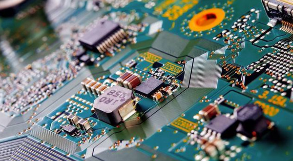
OSP stands for Organic Solderability Preservative. It is an organic surface finish applied to exposed copper areas on a PCB to protect the copper from oxidation and maintain its solderability.
The OSP coating forms a thin protective layer over the exposed copper. During PCB storage and handling, this layer helps reduce oxidation and contamination of the copper surface. During soldering, the coating is displaced or decomposed under the thermal and chemical conditions of the soldering process, allowing the solder to contact the underlying copper surface.
Because OSP does not rely on a relatively thick metallic coating, it provides a very flat surface. This characteristic makes it suitable for PCBs with fine-pitch components and high-density SMT assembly.
How Does the OSP Process Work?
The OSP process involves several controlled chemical treatment steps. The exact process sequence can vary depending on the OSP chemistry and PCB manufacturer's process specifications, but the general workflow includes the following stages.
1. Copper Surface Cleaning
The exposed copper surface is first cleaned to remove contaminants, oxides, and residues that could interfere with the formation of the OSP coating.
Proper surface preparation is important because contamination or oxidation can affect the uniformity and performance of the protective layer.
2. Surface Conditioning
Depending on the OSP chemistry and manufacturing process, the copper surface may undergo conditioning or micro-etching to prepare it for the subsequent organic coating.
This step helps establish a clean and suitable copper surface for consistent OSP film formation.
3. OSP Coating
The prepared copper surface is treated with an OSP solution. The organic compound reacts with the copper surface and forms a thin protective film.
The coating must be sufficiently uniform to protect the copper while maintaining good solderability during subsequent PCB assembly.
4. Rinsing and Drying
After the OSP coating has been formed, the PCB is rinsed and dried according to the process requirements.
Proper control of the process is important to maintain consistent surface quality and prevent contamination or damage to the OSP layer.
5. Inspection and Storage
The finished PCB is inspected to ensure that the surface finish meets the required manufacturing specifications. The boards should then be packaged and stored under suitable environmental conditions to minimize contamination and degradation before assembly.
Advantages of OSP Surface Finish
OSP has several characteristics that make it suitable for modern PCB manufacturing and SMT assembly.
Flat and Uniform Soldering Surface
One of the main advantages of OSP is its very flat surface. Unlike metallic surface finishes that add a metal layer to the copper, OSP forms a thin organic protective coating.
This flat surface can be beneficial for fine-pitch components and high-density SMT assemblies because it provides a relatively uniform interface between PCB pads and component terminals.
Suitable for Lead-Free Assembly
OSP is compatible with lead-free PCB manufacturing and is widely used in lead-free electronics production.
However, being lead-free does not by itself guarantee compliance with every environmental regulation. PCB manufacturers and customers should verify the applicable material and regulatory requirements for the specific project.
Good Solderability
A properly applied OSP coating protects copper from oxidation before assembly while allowing the solder to contact the copper surface during soldering.
This helps maintain consistent solderability when the PCB is manufactured, stored, and assembled under appropriate conditions.
Cost-Effective Surface Finish
OSP generally has a relatively simple material and process structure compared with some metallic surface finishes. This can make it an economical option for applications where its technical characteristics meet the project requirements.
Suitable for Fine-Pitch SMT
Because OSP produces a flat copper surface without the additional thickness associated with plated metallic finishes, it can be well suited to fine-pitch SMT applications.
Limitations of OSP
Although OSP offers several advantages, it is not suitable for every PCB application.
Limited Protection During Handling
The OSP coating is very thin and can be damaged or contaminated by improper handling. Excessive contact, scratching, or contamination of the PCB surface can affect solderability.
For this reason, proper handling, packaging, and storage are important after the OSP process.
Storage Conditions Matter
OSP is intended to protect copper from oxidation, but the coating does not provide unlimited protection under all environmental conditions.
Storage time, temperature, humidity, contamination, and handling conditions can all affect the condition of the surface finish. The manufacturer's recommended storage and assembly requirements should therefore be followed.
Multiple Thermal Exposures Can Be a Consideration
OSP is primarily designed to preserve solderability before assembly. Repeated thermal exposure during multiple soldering operations can affect the surface finish and solderability.
This should be considered when a PCB requires multiple reflow cycles, selective soldering, rework, or other subsequent thermal processes.
Limited Mechanical Protection
Unlike metallic finishes such as ENIG, OSP does not provide a hard metallic surface layer over the copper. Therefore, it should not be selected primarily for applications where the exposed contact surface requires significant mechanical wear resistance.
OSP vs. Other PCB Surface Finishes
OSP is only one of several surface finishes available for PCB manufacturing. The appropriate choice depends on PCB design, assembly process, component requirements, storage conditions, application environment, and cost considerations.
Common PCB surface finishes include:
- OSP: Organic coating over exposed copper; flat surface and commonly used for SMT assembly.
- ENIG: Nickel and immersion gold finish; provides a flat surface and is widely used for demanding PCB applications.
- HASL: Solder coating applied to exposed copper; commonly used and generally cost-effective, although the resulting surface is less flat than OSP or ENIG.
- Immersion Tin: A tin-based metallic surface finish that provides a relatively flat soldering surface.
- Immersion Silver: A silver-based finish offering good solderability and a relatively flat surface.
There is no universally superior surface finish. The correct choice depends on the specific requirements of the PCB and its assembly process.
OSP in SMT Assembly
OSP is commonly used in PCB assembly because it provides a clean and relatively flat copper surface for soldering.
During SMT assembly, solder paste is printed onto the OSP-finished pads before the components are placed. During reflow soldering, the thermal process and flux chemistry allow the solder to wet the underlying copper surface and form the solder joint.
To achieve consistent results, the PCB surface condition, solder paste, stencil design, printing process, and reflow profile should be appropriately controlled.
OSP itself does not compensate for poor solder paste printing or an unsuitable reflow profile. Soldering quality depends on the interaction of the PCB surface finish with the complete SMT process.
Is OSP Suitable for Your PCB?
OSP can be a good choice when a project requires:
- A flat PCB surface for SMT assembly
- Good solderability
- Lead-free manufacturing
- Fine-pitch component assembly
- A cost-effective surface finish
- Compatibility with conventional SMT reflow processes
However, other surface finishes may be more appropriate when the PCB requires exposed contact areas with higher wear resistance, extended storage requirements, multiple thermal cycles, or other specialized performance characteristics.
The surface finish should therefore be selected during PCB design and manufacturing based on the complete application and assembly requirements.
OSP PCB Manufacturing and Assembly at LJPCB
For PCB manufacturers and electronic product developers, surface finish selection should be considered together with PCB fabrication and assembly requirements.
LJPCB provides PCB manufacturing and PCB assembly services, including SMT assembly and other PCB production processes. By evaluating the PCB material, surface finish, component requirements, and assembly process together, manufacturers can select a suitable surface treatment for the intended application.
A properly selected and controlled OSP process can provide a flat soldering surface, protect exposed copper from oxidation before assembly, and support consistent solderability during SMT production.
Conclusion
OSP, or Organic Solderability Preservative, is a widely used PCB surface finish that protects exposed copper from oxidation while maintaining solderability for subsequent PCB assembly.
Its main advantages include a flat surface, good solderability, compatibility with lead-free assembly, and suitability for fine-pitch SMT applications. At the same time, OSP requires appropriate handling and storage because its protective organic coating is thin and can be affected by contamination, mechanical damage, and repeated thermal exposure.
Selecting OSP or another PCB surface finish should be based on the PCB design, component requirements, assembly process, storage conditions, and intended application. When properly specified and manufactured, OSP can provide a practical and reliable surface-finish solution for many modern PCB assemblies.