

What Causes SMT Solder Bridging?
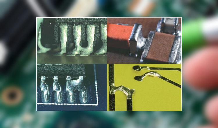
Solder bridging occurs when excess solder forms an unintended connection between two or more adjacent solder pads, component terminals, or leads. This creates an electrical connection where none is intended and may result in short circuits, unstable circuit operation, or even permanent damage to the electronic product.
As electronic products continue to become smaller and more highly integrated, PCB designs increasingly use fine-pitch components and closely spaced pads. This makes precise solder paste printing and component placement more important and can also increase the risk of solder bridging.
Understanding the causes of solder bridging and implementing effective process controls are therefore essential for maintaining PCBA quality and reliability.
Causes of SMT Solder Bridging
Several factors can contribute to solder bridging during SMT assembly.
1. Excessive Solder Paste
Excessive solder paste deposition is one of the most common causes of solder bridging.
During stencil printing, too much solder paste may be deposited on the PCB pads. When the solder paste melts during reflow, the excess molten solder can spread toward adjacent pads and form an unintended connection.
The amount of solder paste depends on factors such as stencil thickness, aperture dimensions, solder paste properties, and printing parameters. Therefore, stencil design and solder paste printing must be carefully controlled, especially for fine-pitch components.
2. Improper Stencil Design
Stencil design has a direct influence on solder paste volume and printing accuracy.
If the stencil apertures are too large, too wide, or not properly designed for the PCB pad geometry, excessive solder paste may be deposited. This can increase the risk of bridging, particularly on fine-pitch ICs and other densely packed components.
Appropriate aperture dimensions, aperture reduction, stencil thickness, and other design parameters should be selected according to the PCB layout and component package.
3. Solder Paste Printing Misalignment
Even when the solder paste volume is appropriate, printing misalignment can cause bridging.
If the stencil is not correctly aligned with the PCB, solder paste may be deposited partially outside the intended pads or too close to adjacent pads. During reflow, the molten solder can then connect neighboring pads.
Accurate stencil-to-PCB alignment and stable printing equipment are therefore essential for consistent solder paste deposition.
4. Component Placement Misalignment
Component placement accuracy can also affect the formation of solder bridges.
If a component is incorrectly positioned during pick-and-place, its terminals may not align properly with the corresponding solder paste deposits. During reflow, molten solder may be drawn toward adjacent terminals or pads, increasing the possibility of bridging.
Regular calibration of pick-and-place equipment and proper control of component placement accuracy can help reduce this risk.
5. Fine-Pitch Components and Small Pad Spacing
As PCB designs become more compact, the distance between adjacent pads continues to decrease.
Fine-pitch components, such as QFPs, SOICs, and other high-density packages, have closely spaced terminals. Even a small amount of excess solder or a slight printing offset can cause two adjacent solder joints to connect during reflow.
For these applications, accurate stencil design and precise solder paste printing are particularly important.
6. Improper Reflow Temperature Profile
An inappropriate reflow temperature profile may also contribute to solder bridging.
The reflow process must provide sufficient thermal energy for the solder paste to melt and wet the intended surfaces while maintaining a stable and controlled process. If the temperature profile is not properly matched to the solder paste and PCB assembly, solder behavior may become inconsistent and defects may occur.
However, solder bridging should not simply be attributed to a "high soldering temperature." Bridging is usually the result of multiple factors, particularly solder paste volume, stencil design, pad geometry, component placement, and process control.
7. Poor Solder Paste Condition
Solder paste properties can also influence printing and reflow performance.
Solder paste that has been improperly stored, used beyond its recommended working life, or handled incorrectly may have inconsistent printing characteristics. Poor paste release from the stencil or unstable deposition can contribute to soldering defects, including bridging.
Solder paste should therefore be stored, prepared, and used according to the manufacturer's specifications.
Solutions to SMT Solder Bridging
To reduce solder bridging in SMT assembly, manufacturers should control the entire process rather than focusing on a single parameter.
1. Optimize Solder Paste Volume
The solder paste volume should be appropriate for the PCB pad and component package. Stencil thickness and aperture dimensions should be carefully selected to achieve the required solder paste deposition.
For fine-pitch components, optimized aperture designs can help control solder volume and reduce the risk of bridging.
2. Optimize Stencil Design
The stencil should be designed according to the PCB layout, pad geometry, component pitch, and solder paste requirements.
Proper aperture dimensions and reductions can help prevent excessive solder paste from being deposited between closely spaced pads.
3. Improve Printing Accuracy
The solder paste printing process should be properly controlled to maintain consistent paste volume and alignment.
Parameters such as printing speed, squeegee pressure, stencil condition, and PCB-to-stencil alignment should be regularly checked and optimized. Regular stencil cleaning is also important because blocked or contaminated apertures can affect solder paste deposition.
4. Maintain Accurate Component Placement
Pick-and-place equipment should be regularly maintained and calibrated to ensure accurate component positioning.
Correct component alignment helps ensure that component terminals remain properly positioned over the solder paste deposits during reflow, reducing the risk of bridging.
5. Optimize the Reflow Profile
The reflow temperature profile should be established according to the solder paste manufacturer's specifications, PCB design, and component requirements.
The preheat, soak, reflow, and cooling stages should be properly controlled to ensure consistent solder melting and wetting. The actual temperature profile should also be verified periodically to ensure that the reflow oven remains within the required process conditions.
6. Maintain SMT Equipment
Regular maintenance and calibration of solder paste printers, pick-and-place machines, and reflow ovens are essential for stable SMT production.
Equipment problems can lead to printing misalignment, inconsistent paste deposition, inaccurate component placement, or unstable thermal profiles, all of which can increase the risk of solder bridging.
Conclusion
SMT solder bridging is a common PCB assembly defect in which excess solder unintentionally connects adjacent pads or component terminals. It can result in electrical shorts, unstable circuit operation, and reduced product reliability.
Common causes include excessive solder paste, improper stencil design, printing misalignment, component placement errors, fine-pitch component layouts, unsuitable reflow profiles, and inconsistent solder paste conditions.
Effective prevention requires comprehensive process control, including optimized stencil design, accurate solder paste printing, precise component placement, proper reflow profiling, and regular SMT equipment maintenance. By controlling these factors throughout the SMT assembly process, manufacturers can significantly reduce solder bridging and achieve more consistent and reliable PCBA quality.