

PCB Immersion Gold Process: ENIG Benefits and Limitations
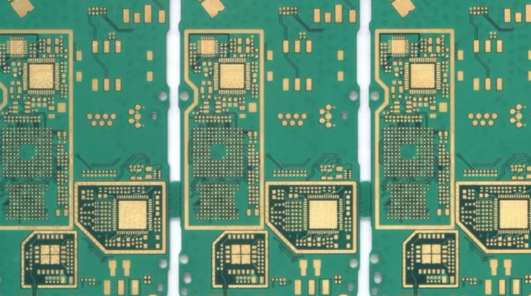
What Is the PCB Immersion Gold Process? A Guide to ENIG
In PCB manufacturing, immersion gold usually refers to electroless nickel immersion gold (ENIG), a surface finish applied to exposed copper pads before assembly. It consists of a nickel layer covered by a thin gold layer.
ENIG protects solderable surfaces and provides a flat finish for component attachment. It is commonly selected for fine-pitch SMT assembly, but its suitability depends on the board’s electrical, mechanical, and manufacturing requirements.
What Is an ENIG Surface Finish?
ENIG stands for electroless nickel immersion gold. Its basic layer structure is:
Copper pad → Electroless nickel → Immersion gold
The nickel acts as a diffusion barrier between the copper and gold and provides the underlying surface for solder joint formation. The thin gold layer protects the nickel from oxidation before assembly.
During soldering, the thin gold coating dissolves into the molten solder, allowing the solder to react with the underlying nickel. The finished connection therefore should not be understood as solder simply adhering to a permanent gold film.
ENIG is applied during bare PCB fabrication. It prepares the board for subsequent assembly rather than replacing any soldering operation.
How Does the PCB Immersion Gold Process Work?
1. Surface Cleaning and Preparation
The exposed copper is cleaned to remove contamination and prepared for uniform deposition. Controlled microetching and activation are typically included, depending on the selected process chemistry.
Surface preparation is critical. Contamination or inconsistent activation can lead to incomplete coverage or other plating defects.
2. Electroless Nickel Deposition
The board enters an electroless nickel bath. A chemical reducing agent drives nickel deposition on the activated surface without an external electrical current.
Conventional ENIG processes deposit a nickel-phosphorus alloy. Bath composition, temperature, pH, and processing time must be controlled to achieve the required deposit characteristics.
3. Immersion Gold Deposition
The nickel-coated board is immersed in a gold-containing solution. In conventional immersion gold chemistry, a displacement reaction deposits gold while a small amount of nickel dissolves.
This differs from both electrolytic gold plating and the reducing-agent-driven deposition used in the nickel stage. The conventional immersion reaction is largely self-limiting as gold covers the nickel surface.
Commercial gold bath chemistries vary, so the fabricator must follow the qualified process rather than assume all systems operate identically.
4. Rinsing, Drying, and Inspection
Rinsing between stages limits chemical carryover. After finishing, the board is rinsed, dried, and inspected.
Quality checks may include deposit thickness measurement, coverage inspection, solderability evaluation, and assessment of nickel corrosion. A uniform gold appearance alone does not demonstrate acceptable finish quality.
Main Benefits of ENIG
Flat Pads for Fine-Pitch Assembly
ENIG provides a relatively flat surface without the solder thickness variation associated with hot air solder leveling (HASL). This makes it useful for fine-pitch components and packages such as BGAs and QFNs.
Flatness supports assembly consistency, but pad design, stencil printing, placement, and reflow control remain essential.
Protection Before Soldering
The gold layer helps preserve the underlying nickel surface until assembly. This supports solderability during storage when the boards are packaged and handled according to the supplier’s instructions.
Storage life is not unlimited. It depends on finish quality, packaging, environmental exposure, and handling.
Deposition Without Electrical Plating Connections
ENIG does not require each pad to be connected to an external plating circuit. This allows the finish to be deposited on isolated conductive features, provided they are properly prepared and accessible to the process chemistry.
ENIG vs. Electroplated Hard Gold
Immersion gold and electroplated gold are different processes. “Electrolytic immersion gold� is not an appropriate category for explaining conventional PCB finishes.
| Feature | ENIG | Electroplated hard gold |
|---|---|---|
| Deposition method | Electroless nickel followed by immersion gold | Gold deposited using an external electrical current, typically over nickel |
| Main purpose | Preserve solderability and provide a flat assembly surface | Provide durable electrical contact surfaces |
| Typical use | Component solder pads | Edge connectors and contacts subject to repeated mating |
| Wear resistance | Thin gold layer is not intended for repeated sliding wear | Hard gold is selected for greater resistance to contact wear |
A PCB can use ENIG on solder pads and selective hard gold on connector fingers when the fabrication process supports both. These are specified finishes for different areas, rather than interchangeable coatings.
Limitations and Quality Risks
Nickel Corrosion and Black Pad
Excessive nickel corrosion during gold deposition can contribute to the defect commonly called “black pad.� It can compromise solderability or produce a weak, brittle solder joint interface.
Not every dark pad is evidence of black pad, and external appearance alone is insufficient for diagnosis. Process control and appropriate analysis are necessary. Eurocircuits identifies black pad and interface embrittlement among the potential risks of ENIG processing.
Cost and Process Complexity
ENIG generally costs more than finishes such as OSP because it requires multiple chemical stages, gold chemistry, and close process monitoring.
Its value should be assessed against assembly requirements rather than appearance alone.
High-Frequency Performance
ENIG does not automatically improve signal integrity. The nickel layer can increase conductor loss in high-frequency circuits, particularly where finished conductors carry RF signals.
The effect depends on frequency, transmission-line geometry, and the extent of finish coverage. RF and microwave designs should evaluate the finish as part of the electrical design.
When Should You Choose ENIG?
ENIG is worth considering when a design needs flat solder pads, fine-pitch assembly capability, and a protective finish compatible with the planned manufacturing process.
It may be used in communications, industrial, medical, and other electronic products, but an industry label alone does not establish suitability. High-reliability applications still require appropriate materials, process qualification, inspection, and product testing.
For repeated-contact wear, evaluate hard gold. If wire bonding is required, assess the wire material and bonding process; ENEPIG may be a suitable alternative for some applications, but it is a distinct nickel-palladium-gold finish.
Before ordering, agree with the PCB manufacturer on the finish specification, deposit thickness requirements, solderability criteria, storage conditions, and any special electrical or mechanical constraints. ENIG should be selected to meet those requirements, not simply because the pads look gold.