

PCB Immersion Tin: Process, Benefits, and Limitations
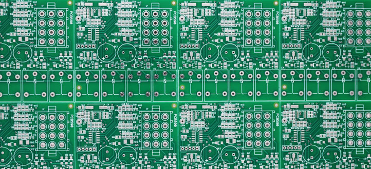
What Is PCB Immersion Tin? Process, Benefits, and Limitations
PCB immersion tin is a surface finish that deposits a thin layer of tin directly onto exposed copper through a chemical displacement reaction. Also called immersion tin plating or ISn, it protects solderable copper surfaces before assembly and provides a flat finish for component attachment.
Immersion tin can support SMT, through-hole soldering, and qualified press-fit applications. Its performance depends on deposit quality, storage conditions, and the assembly process. It should not be described as a finish that eliminates intermetallic growth or tin whisker risk.
How Does the Immersion Tin Process Work?
During immersion tin processing, the PCB enters a chemically controlled bath containing dissolved tin species and other constituents. Tin deposits on exposed copper while some copper dissolves into the solution. No external electrical current is required.
Complexing chemistry makes the displacement process possible under the selected bath conditions. It is not a reaction in which a tin oxide converts the copper surface into tin and releases oxygen.
Process supplier Uyemura describes immersion tin as selective deposition on copper through displacement. Uyemura: Immersion Tin Processes
Unlike electroplated tin, immersion tin does not require the individual pads to be electrically connected to a plating power supply. Unlike hot air solder leveling (HASL), it does not involve dipping the board into molten solder and leveling the coating with hot air.
Main Steps in PCB Immersion Tin Processing
1. Cleaning and Surface Preparation
The exposed copper must be free of oils, fingerprints, and residues that could interfere with deposition.
The cleaning chemistry must be compatible with the board materials and solder mask. A generic acid-cleaning recipe should not replace the chemical supplier’s approved process.
2. Controlled Microetching
Microetching removes a small amount of surface copper to produce a clean, consistent surface for finishing.
This is a surface preparation step, not the main circuit-pattern etching operation. Excessive microetching can affect fine features, so copper removal must remain within the qualified process limits.
3. Predip or Conditioning
Where required by the process, a predip conditions the copper surface and helps control the chemistry carried into the tin bath.
The formulation and sequence are specific to the selected system. A proprietary product code should not be presented as a universal requirement for immersion tin.
4. Immersion Tin Deposition
The prepared board enters the tin bath. Temperature, dwell time, bath composition, and solution movement are controlled to achieve the specified finish.
Monitoring must account for chemical consumption and the accumulation of dissolved copper and other by-products. Replenishment alone does not guarantee unlimited bath life.
5. Rinsing, Drying, and Inspection
The finished board is rinsed according to the process requirements and dried before packaging.
Inspection should assess coverage, surface condition, thickness, and solderability. Appropriate measurement methods are important because the condition of the tin layer changes as copper and tin interact.
Advantages of Immersion Tin
Flat Pads for SMT Assembly
Immersion tin provides a relatively flat surface without the solder thickness variation associated with HASL. This makes it useful for fine-pitch component footprints.
Flatness supports consistent assembly, but it does not prevent solder bridging by itself. Pad spacing, stencil design, paste printing, and component placement remain critical.
Compatibility with Qualified Lead-Free Processes
Suitable immersion tin systems can support lead-free assembly and multiple soldering operations. Atotech identifies its Stannatech 2000 process for multiple lead-free soldering and press-fit applications. That capability should be qualified for the actual board and production sequence rather than assumed for every immersion tin finish. Atotech: Final Finishing Technologies
No Precious-Metal Layer
Immersion tin does not require gold or palladium, which can make it a cost-effective alternative to precious-metal finishes.
However, its total cost is not universally equal to HASL or a fixed amount below ENIG. Pricing depends on board design, production volume, process capability, inspection, and handling requirements.
Options for Flexible Circuits
Immersion tin is not limited to rigid boards. Process suppliers offer formulations developed specifically for flexible substrates, with attention to material compatibility and deposit uniformity.
For example, Atotech’s Stannatech-Flex is designed for flex applications. This does not mean that every immersion tin chemistry is suitable for every flexible circuit construction. Atotech: Stannatech-Flex Technical Overview
Limitations and Reliability Considerations
Copper–Tin Intermetallic Growth
Copper and tin react at their interface, forming intermetallic compounds. This interaction continues during storage and is accelerated by thermal exposure.
As the intermetallic layer grows, the amount of unreacted tin available for soldering decreases. Initial coating thickness alone therefore does not describe the board’s solderability after storage or repeated heating.
IPC’s public immersion tin specification excerpt explicitly recognizes copper–tin diffusion and its effect on shelf life and finish performance. IPC-4554 with Amendment 1: Public Excerpt
Tin Whisker Risk
Immersion tin must not be advertised as inherently whisker-free. Tin whiskers are conductive filaments that can grow from susceptible tin surfaces and potentially bridge nearby conductors.
NASA identifies intermetallic formation and associated stresses among the factors involved in tin whisker growth. Mitigation measures can reduce risk, but they should not be treated as a universal guarantee. NASA: Basic Information Regarding Tin Whiskers
Storage and Thermal Exposure
Use the PCB supplier’s specified shelf life, packaging, and storage conditions. Avoid direct contact with solderable surfaces and unnecessary exposure to contamination.
The intended assembly sequence should include all reflow passes, subsequent soldering operations, and expected rework. Pads that remain unsoldered through earlier heating cycles require particular attention.
Baking should follow a finish-compatible procedure. It is not a general method for restoring aged immersion tin solderability.
Press-Fit Qualification
Immersion tin can be used in approved press-fit applications, but compatibility depends on the connector system, finished hole dimensions, plating, and insertion conditions.
IPC also identifies whisker concerns associated with insertion-induced stress. Follow the connector manufacturer’s requirements and the applicable product qualification plan. IPC-4554 with Amendment 1: Application Considerations
Is Immersion Tin Environmentally Friendly?
Immersion tin can support lead-free manufacturing, but “lead-free� does not mean pollution-free.
The process uses chemical solutions and generates metal-containing waste streams. Chemical handling, rinsing, bath maintenance, and waste treatment must follow the relevant supplier instructions and facility requirements.
Claims such as “fluorine-free� or “fully recyclable� require evidence for the specific chemistry and waste-management process. They should not be presented as universal properties of immersion tin.
What Should You Specify Before Ordering?
Agree with the PCB manufacturer on the applicable finish specification, thickness requirements, measurement method, solderability criteria, storage conditions, and assembly sequence.
For multiple soldering operations or press-fit connections, request evidence relevant to the intended application. Do not use a generic thickness range as proof of process durability.
Immersion tin is a practical option when a flat, solderable finish fits the product’s needs. Successful use depends on controlling deposit quality and preserving solderability through storage and assembly.