

The difference between PCB electroplating gold and immersion gold?
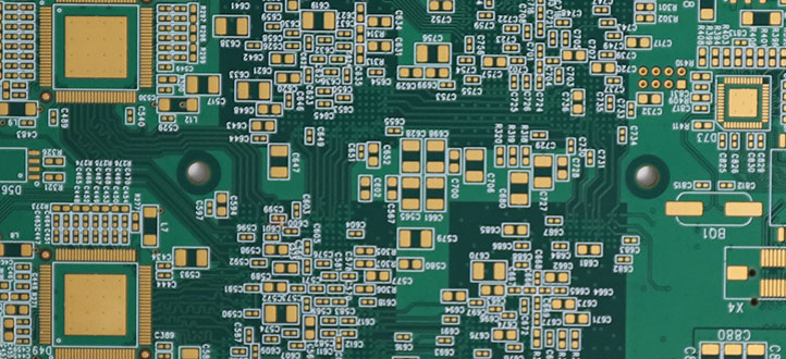
Electroplated Gold vs. ENIG: Which PCB Finish Should You Choose?
Electroplated gold and immersion gold can both produce gold-colored PCB surfaces, but they differ in deposition method, design requirements, and intended use.
Electroplated gold uses an external electrical current and can be specified as hard or soft gold. PCB immersion gold usually refers to electroless nickel immersion gold (ENIG), a chemically deposited nickel-and-gold finish commonly used to preserve solderability.
The right choice depends on whether the surface will be soldered, wire bonded, or used as a mechanical contact.
How Do the Two Processes Work?
Electroplated Gold
Electroplating uses electrical current to deposit gold onto conductive features connected to the plating circuit. Nickel is commonly deposited first as an underlayer between copper and gold.
The gold deposit can be engineered for different properties. Hard gold is commonly selected for contact wear resistance, while high-purity soft gold may be specified for qualified bonding applications. Process suppliers offer distinct electrolytic nickel, soft-gold, and hard-gold systems. Technic: Electrolytic Precious-Metal Processes
Immersion Gold: ENIG
ENIG uses two different chemical deposition steps. Electroless nickel is deposited onto prepared copper, followed by a thin gold layer formed through an immersion process.
The nickel provides a diffusion barrier, while gold protects the nickel before assembly. Umicore describes ENIG as a flat, solderable finish applied to the surfaces and vias intended to receive it. Umicore: ENIG Process
No external plating current is required. However, it is inaccurate to describe the entire ENIG sequence as a single displacement reaction: nickel deposition and immersion gold deposition use different reaction mechanisms.
Electroplated Gold vs. ENIG at a Glance
| Factor | Electroplated gold | ENIG |
|---|---|---|
| Deposition method | External current drives gold deposition | Electroless nickel followed by immersion gold |
| Electrical access | Each plated feature needs a current path | No external electrical connection to each pad |
| Gold properties | Hard or soft gold according to the specification | Thin protective immersion gold layer |
| Common applications | Connector fingers, contact areas, and qualified bonding pads | Solder pads and other qualified connection surfaces |
| Repeated sliding wear | Hard gold can be specified for this purpose | Not a substitute for a qualified hard-gold contact finish |
| Coverage | Defined by masking, electrical access, and process design | Defined by exposed, prepared surfaces and process design |
| Cost drivers | Gold thickness, plated area, tooling, and process requirements | Finished area, chemistry, process control, and inspection |
Key Differences in PCB Design and Manufacturing
1. Electrical Connections and Layout Constraints
Electroplating requires an electrical path to the features being plated. Temporary connections or plating buses may be needed, depending on the fabrication method.
The designer and fabricator should agree on how these connections will be provided and subsequently removed or isolated. Any remaining conductive features must also be compatible with the electrical design.
ENIG does not require these external plating connections. Electrically isolated pads can receive the finish when their surfaces are correctly prepared and accessible to the process chemistry.
2. Selective Coverage
Electroplated gold is often applied selectively to connector fingers or other defined contact areas.
ENIG does not coat the entire PCB indiscriminately. It is normally deposited on exposed conductive surfaces prepared for finishing, not on solder mask or the insulating laminate.
A board may combine ENIG solder pads with selectively electroplated hard-gold fingers. This requires a fabrication process that supports both finishes and clearly identifies their respective areas.
3. Gold Thickness and Uniformity
Electroplating offers flexibility in deposit thickness, but the required thickness depends on the application. Contact wear, bonding requirements, porosity, and cost all influence the specification.
ENIG uses a thin gold layer primarily to protect the underlying nickel. Its thickness must also be controlled; “thin� does not mean that thickness is unimportant or unmeasurable.
Avoid applying a universal thickness range to every electroplated-gold or ENIG design. Specify the applicable requirements, measurement method, and acceptance criteria with the manufacturer.
Electroplated thickness distribution is influenced by current distribution and feature geometry. ENIG coverage and uniformity depend on preparation, chemistry, and process control. Neither method automatically guarantees a flawless deposit.
Soldering, Wire Bonding, and Contact Wear
Soldering and Gold Embrittlement
During soldering, gold dissolves into the molten solder. Excessive gold in a susceptible solder system can contribute to brittle gold-containing intermetallics and reduced joint reliability. The Aerospace Corporation discusses this failure mechanism in its guidance on excessive gold in soldered connections. The Aerospace Corporation: The Pitfalls of Too Much Gold
A thicker coating can introduce more gold for the same plated area, but risk also depends on solder volume, alloy, and contributions from other gold-finished surfaces.
ENIG’s thin gold layer helps limit the amount introduced, but it does not justify describing the finish as immune to gold embrittlement. Hard gold intended for contact wear should not automatically be used on solder pads.
Wire Bonding
Soft electroplated gold may be appropriate for wire bonding when purity, hardness, thickness, and cleanliness meet the bonding process requirements.
ENIG can support certain qualified bonding applications, but it should not be assumed interchangeable with a specified soft-gold finish. Select the metallization according to the wire material and bonding method.
Repeated-Mating Contacts
For connector fingers exposed to repeated insertion and removal, electroplated hard gold is generally the more relevant option.
Contact life depends on the complete system, including the mating contact, normal force, coating thickness, and operating environment. A gold-colored appearance alone says little about wear performance.
Cost and Quality Considerations
Electroplated gold can be expensive when a large area or substantial gold thickness is required. Selective plating can reduce precious-metal usage, although masking and electrical-access requirements add manufacturing work.
ENIG also involves multiple chemical stages and close process control. It should not automatically be described as simpler, faster, or cheaper for every board.
Quality risks also differ. ENIG requires control of nickel corrosion, while electroplated finishes require attention to current distribution, adhesion, porosity, and deposit properties. IPC’s ENIG specification includes nickel corrosion and corrosion-performance monitoring among its covered subjects. IPC-4552B: Official Public Contents
Compare quotations against the same functional requirements rather than comparing finish names alone.
Which Finish Is Right for Your PCB?
For conventional soldered SMT connections, ENIG is often a practical option when flatness and surface protection are priorities.
For repeated-mating contacts, evaluate electroplated hard gold. For wire bonding, specify a finish qualified for the actual bonding process rather than requesting generic “gold plating.�
Some designs benefit from using different finishes in different areas. Before production, identify each surface’s function and agree on coverage, deposit requirements, electrical-access provisions, and inspection criteria.
When discussing a project with LJPCB, include the fabrication files, intended assembly process, and any connector or bonding requirements. These details provide a clearer basis for a surface-finish discussion than gold appearance alone.